SUPER BOARD
This is a joint project between Ed and Marcel.
To better explain the project, each of us will use a different text color it indicate who's comments you are reading.
Ed's text is in this color.
Marcel's text is in this color.
BACKGROUND
In April of 2012 I completed construction of a COSMAC VIP II computer that I designed. You can read about it here:
http://www.cosmacvip.com/VIP2/VIP2.php
Late May 2012
Not long after that project was completed, I was contacted by Marcel van Tongeren. Marcel is the developer of EMMA 02, an emulator that specializes in 1802 based systems. It is a really awesome emulator that can be found here:
http://www.emma02.hobby-site.com/index.html
Marcel and I exchanged e-mails for a few weeks regarding my VIP II and other 1802 based systems. I asked him if he had any experience with the COMX-35 computer. He indicated that it was his favorite 1802 based computer. Marcel and his brother were prolific developers for the COMX-35. You can read more about them here:
http://www.emma02.hobby-site.com/comx_fandm.htm
Middle of June
Marcel gave me contact information for someone in Finland who in the past had a few brand new COMX-35 systems he was selling. I contacted this person and waited for a response.
While waiting for a response, a single used COMX appeared on eBay. So I bid on it and won. Not long after this I was happy to hear that the person in Finland actually had a few systems left for sale, so I made arrangements to make a purchase.
The system from Finland arrived first. The used system was coming in from Indonesia and took 6 weeks to arrive.
Good thing I followed through on the Finland purchase as the used system did not work. Someone had tried to repair it and delaminated the PCB.
It would power up but had no function. Not all was lost with it however; I used this dead board to draw up a full schematic of the COMX-35 from which I built a complete COMX-35 system. You can read about that project here:
I was curious what information was available for the COMX. Marcel pointed me to a page for it on the Emma 02 website:
http://www.emma02.hobby-site.com/index_comx.html
He also suggested the COMX-Club website:
http://www.comxclub.hobby-site.com/COMX-Club.htm
which is run by Dennis in the Netherlands.
RESEARCH
First week of July
The COMX from Finland arrived. It was brand new!
The COMX has a PAL modulator built in that transmits on TV channel 36. I have a PAL monitor but not a PAL TV. The first thing I needed to do was open the COMX and find the video signal as it entered the modulator. After I found it, I added a short cable with a female RCA connector on it. This allowed me to connect the COMX to my monitor. This worked out great.
Marcel asked if it would be possible to add an IDE interface to the COMX. I responded that just the night before I had been thinking about whether I could add a USB key interface to the COMX.
At this time I had also just ordered a 'new' COMX from our contact in Finland, I thought it would be nice if there was a way to easily access the SW library for the COMX. Of course without tapes and multiple floppy disks.
We exchanged a bunch of messages, and in the end, the IDE card and USB key ideas became a USB interface card.
Marcel and I decided that he would handle all of the firmware/software development and I would do all of the hardware design/prototyping. The only real issue we would need to work around was when we could be online at the same time because Marcel lives in Sweden and I live in the US. As it turned out this was not a problem at all.
I started work on the hardware.
Yes I offered to write all firmware and PC software, however I had not written any real 1802 code for about 25 years!
Sure I had worked with Emma 02 for years so I did have a reasonable good knowledge of the 1802 and COMX Hardware. However I didn't have a clue how I should go about this, what assembler to use, should I use the floppy controller firmware as base or the network card firmware or maybe just start from scratch?
At the time I was in the process of adding a 'direct assembler' to Emma 02, mainly targeting a tool to allow changing existing code. Still I decided that using this tool with some additions could be very good for writing some small firmware. I expected it would never go any larger than 8K anyway if it would even reach that!
Now when we are almost ready the firmware including some existing code like Tennismania and Eat a worm is close to 68K.
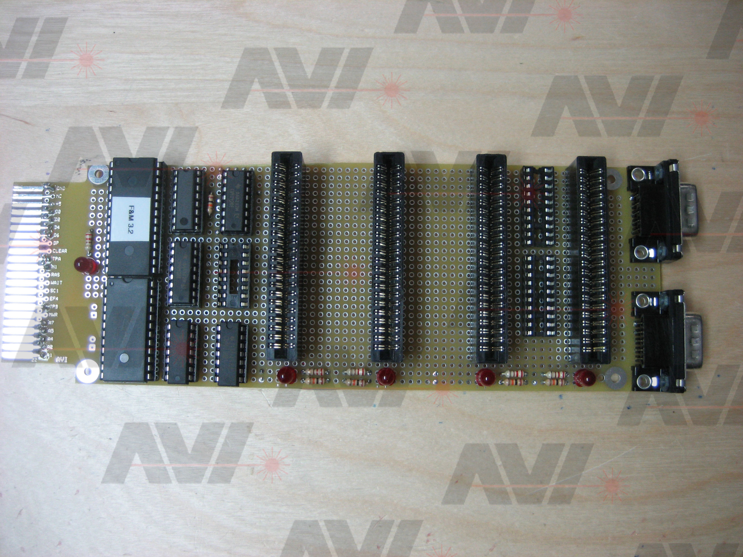
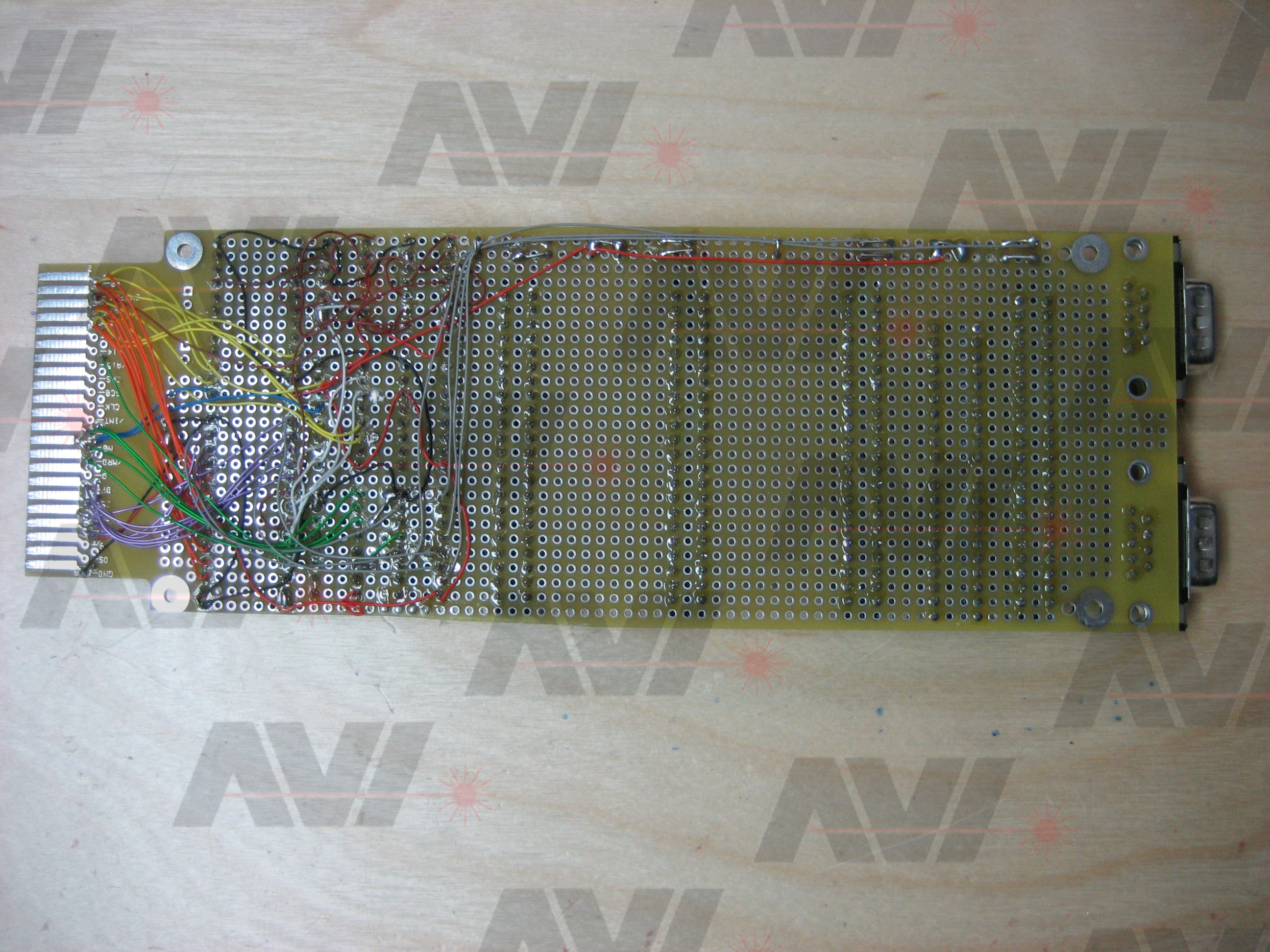
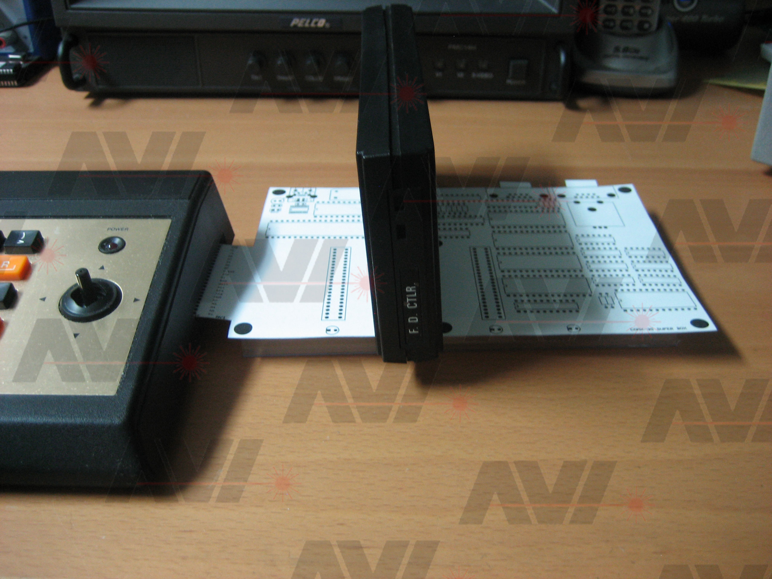
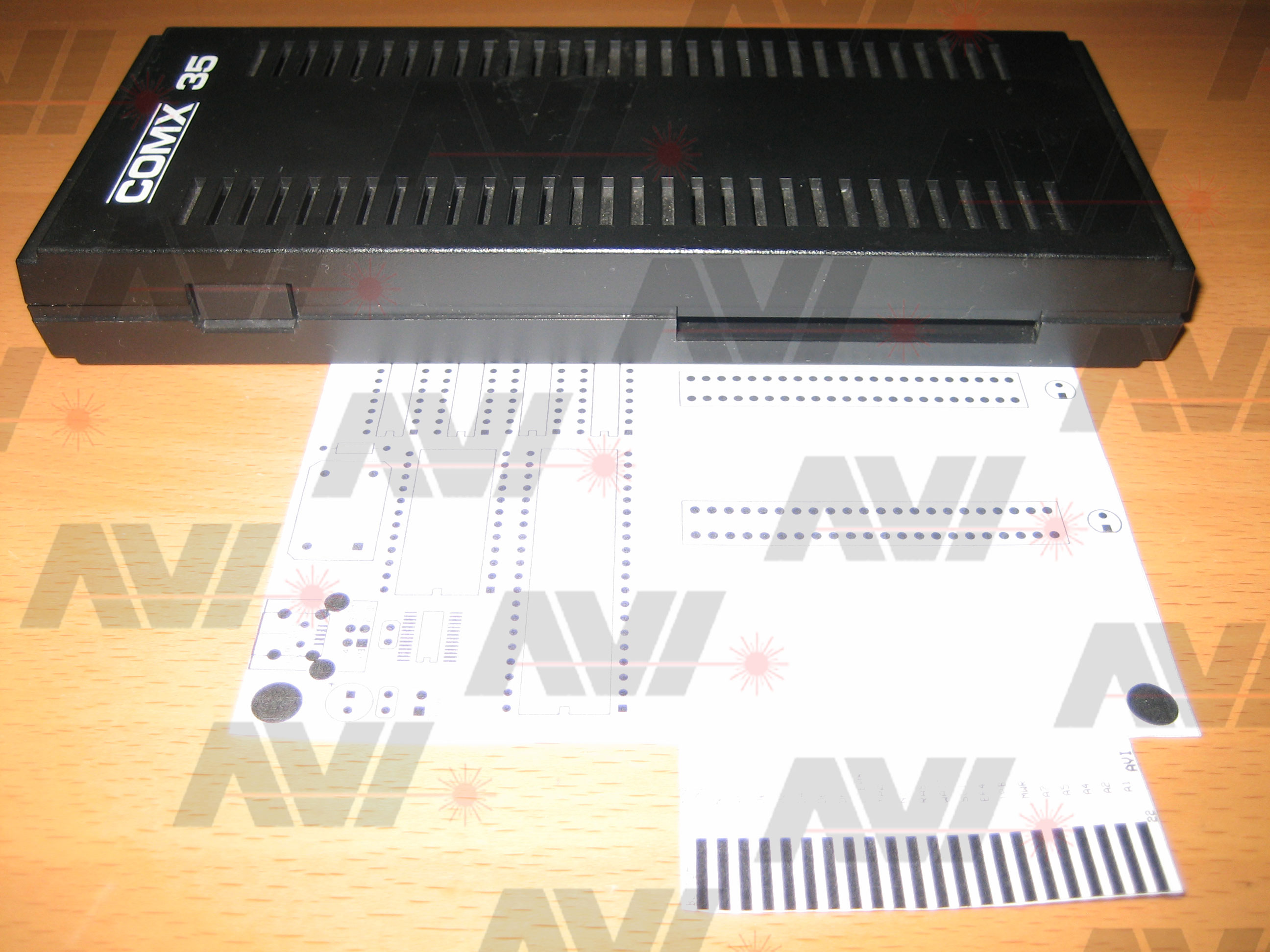
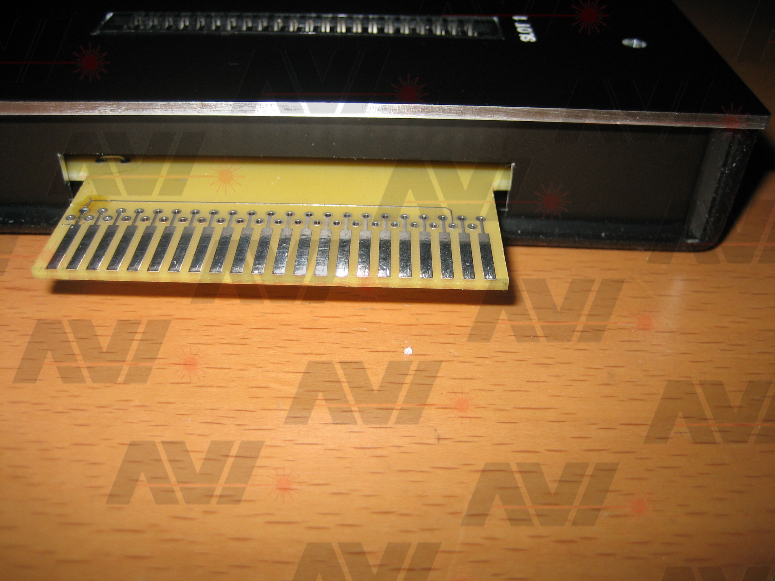
I started by designing a simple interface board for the COMX, using the "COMX Technical Manual". (http://www.comxclub.hobby-site.com/COMX35TechnicalManual.pdf)
Here is a picture of the board:
It is designed to be installed like a normal interface card, facing towards the back of the COMX, or straight out the side. I did this to give myself options.
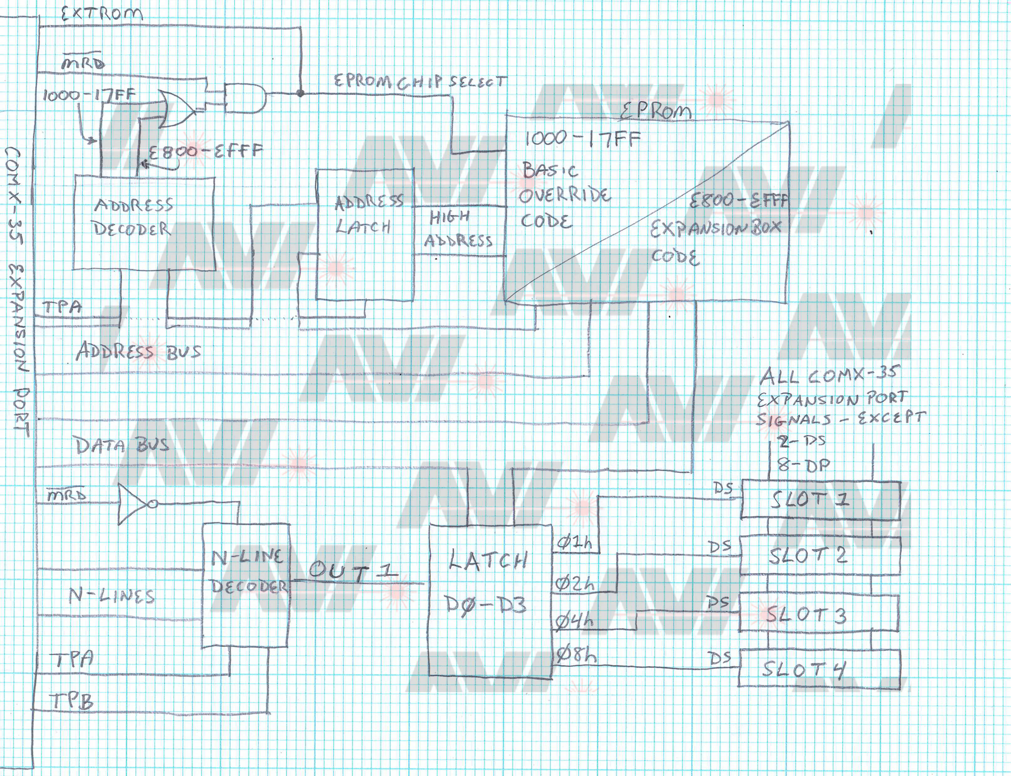
In order to get something working, I read through the "COMX Expansion Box Manual"(http://www.comxclub.hobby-site.com/expansionboxmanual.pdf), focusing on the circuit description on page 7. From this, and a bunch of other reading, I was able to build a functioning expansion box. Here is a block diagram of it:
Here is what I built:
I was just interested in getting something to run so I did not wire up the actual slot connectors, other than the /DS line (Device Select).
USB CARD
Using the information I had gained designing the expansion box, I began working on an address decoder that would enable use of the C000h-DFFFh area in memory. The COMX was developed with this memory space empty for hardware developer use. There is also a small area located at F000h-F3FFh that is also available. I made use of that also later in the project.
After a bit I came up with a design that I thought would work. I created a PCB for the USB card.
- It contained these sections:
- - Address latch - To decode the high addresses (A8-A15) of the 1802 contained in the COMX
- - N-line decoder - To address I/O requirements
- - LED driver - COMX expansion cards have two LEDs, "Select" and "Active"
- - UART - Used to convert the parallel data on the 102 data bus to serial
- - Baud rate generator- To provide the proper timing for the UART
- - USB interface - Used to convert the serial data from the UART to a valid USB signal.
Third week of July
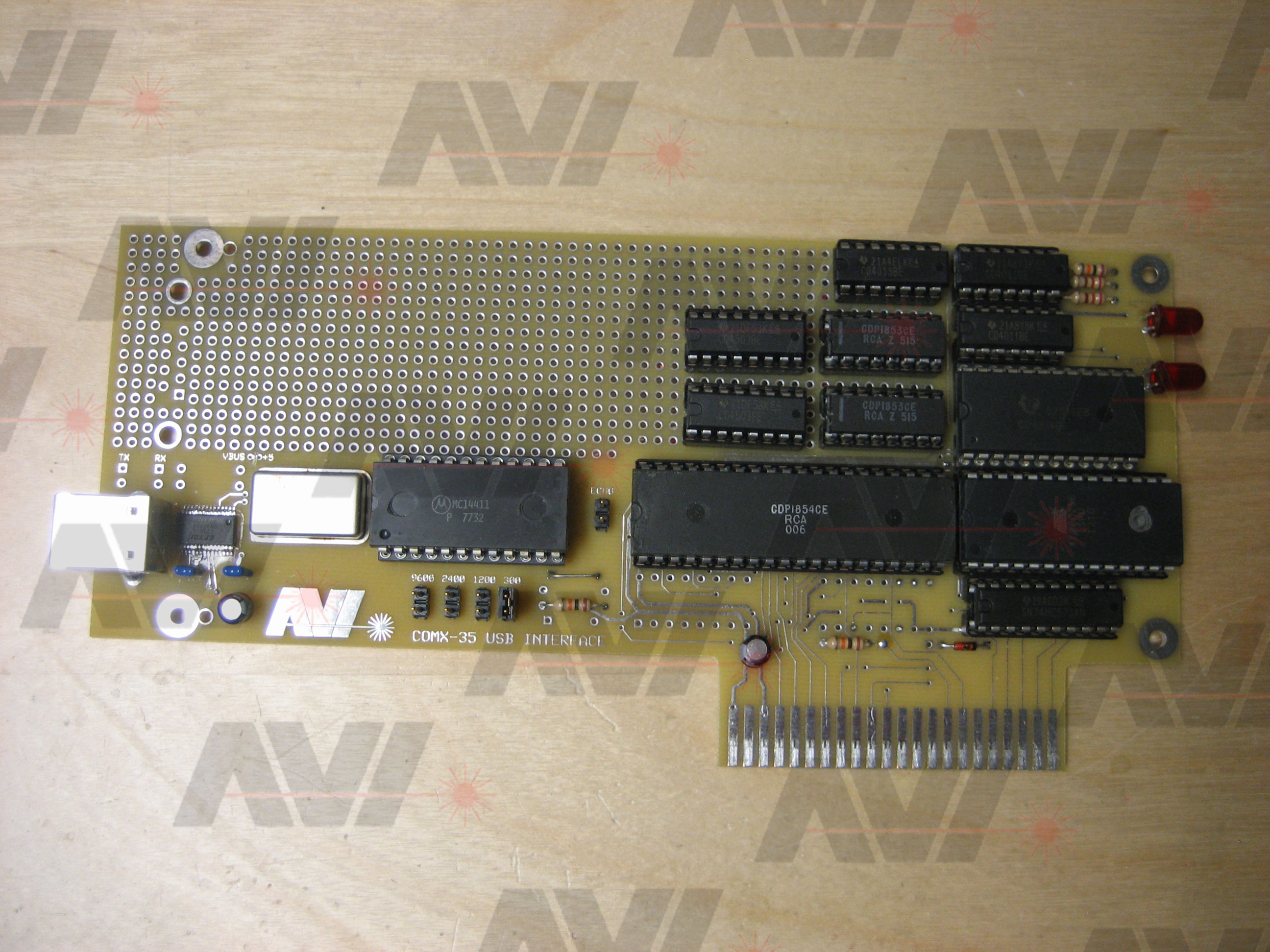
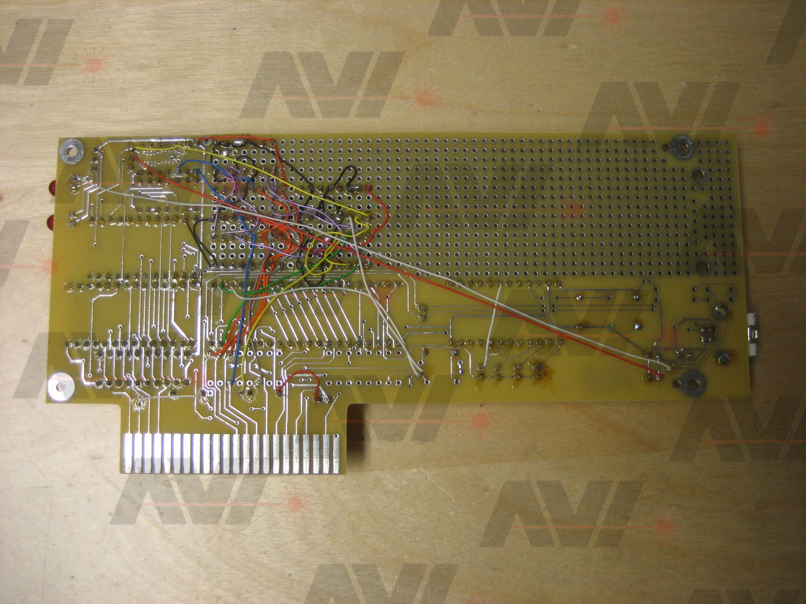
Here are some pictures of the board:
Since firmware for the USB card had not been written yet, I used the EPROM code from the Thermal Printer card to test the address decoder. I was able to access the memory dump routine at C0C0h of the thermal printer ROM. So the address decoder and latch seemed to be working.
The code for the Thermal printer EPROM is included with the Emma 02 emulator.
I also tested the LED drivers. The "Selected" LED indicates that this board is the one currently selected. When just installed in the side of the COMX, it is always illuminated. When a board is installed in the COMX expansion box, the LED indicates that the slot the board is installed in is the currently selected slot. If a different slot is active, this LED is extinguished. The "Active" LED is illuminated when the EPROM on the USB card is accessed. Both LEDs worked as they should.
I then did a loop back test to make sure the USB section was working. I used the popular FTDI Serial-to-USB interface chip, so the driver was already installed on my PC (Windows 7-64bit). I had placed a shorting block on the PCB just for loop back testing:
I placed a shunt over these pins so anything sent from the PC would be echoed back if the USB section was correct. Using a terminal program on my PC, I selected the correct comport and began typing. At this point baud rate, start, stop and data bits don't matter. Whatever is sent gets echoed back. As I typed I could see the same characters received by the PC indicating the USB interface was working correctly. The PCB also has two LEDs, one for receive and one for transmit. These were both blinking as expected.
Next I tested the baud rate generator. I put four baud rate selection jumpers on the PCB:
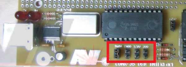
These allowed for selection of baud rates: 300, 1200, 2400 and 9600
I used the MC14411 baud rate generator chip with a 1.8432MHz full size oscillator because I had some on hand. Using my oscilloscope, I tested to make sure that the 4 rates were correct and they were.
The UART section would need firmware, so it would have to wait. I wrote up some information for Marcel so he could start researching the needed firmware.
With the details Ed provided to me about his hardware design, I started to write some code in Emma 02 to emulate the USB card as well as emulate the future PC communication software. This would allow me to write and test a lot of the firmware without having my hands on a real board.
I decided to write the firmware from scratch as there were no similarities to any existing hardware or firmware.
For test purposes both for Ed and myself (and based on some code I received from Ed) I made some small routines that could send/receive 256 bytes of data. This was our first firmware build, now we are working on build 135 almost 13 months later!
To allow for some kind of real commands instead of CALLs to machine code I planned to design the command handling via the expansion board firmware.
This would allow for using the 'CARD Sx' command when an expansion box was used and a 'CALL(@C010)' command when the USB card was plugged directly into the COMX. It would also allow for adding a new command, 'USB', if the expansion box ROM was replaced with a new version.
COMX Basic had 2 unused commands 'TOUT' and 'POUT'. One was replaced by the expansion box firmware with the 'CARD' command. The other was available for 'USB'.
Focus I had was to get basic load and save commands working and then add some directory commands. The plan was to develop the following commands:
- - CARDS1 PSAVE,FILENAME
- - CARDS1 PLOAD,FILENAME
- - CARDS1 CAT
- - CARDS1 CHDIR,DIRECTORY
On the PC side we chose to use the Emma 02 .comx format. All available COMX software was already stored in .comx files and it would make it easy to share files between the COMX and Emma 02 as well.
I then began testing the N-line decoders. I needed to have a working "OUT2" and "INP2" as these are available on the COMX. The decoder is formed by two chips:
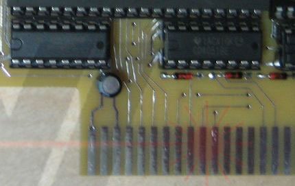
Something was wrong. I did not see pulses when I issued either an "OUT" or "INP" instruction. I could see activity on the N-lines themselves, indicating that the command was run. The problem was in my circuit. I tried a lot of different things, but it was obvious I had messed up this section.
As I was hoping to get actual hardware in Marcel's hands as soon as possible so he could more easily test his firmware, I decided to not debug my N-line decoder design. I decided to install an actual N-line decoder chip. Since I have a handful of CDP1853s, that is what I used. For now I only installed one to handle "OUT"s. I made a bunch of cuts on the PCB and point to point wired in a CDP1853. I then got the correct pulses for the "OUT" instruction.
Marcel provided me some UART specific firmware to test with. It was only for sending from the COMX to the PC, but it worked great!
I rewired the CDP1853 so it would act as an input decoder. At this point there is no software on the COMX yet to do anything with received data. When I typed a single character on the PC, I saw the data arrive on my scope.
I have two logic analyzers, an 8 channel and a 16 channel. I hooked it up the 16 channel to the UART to see the value of the data received.
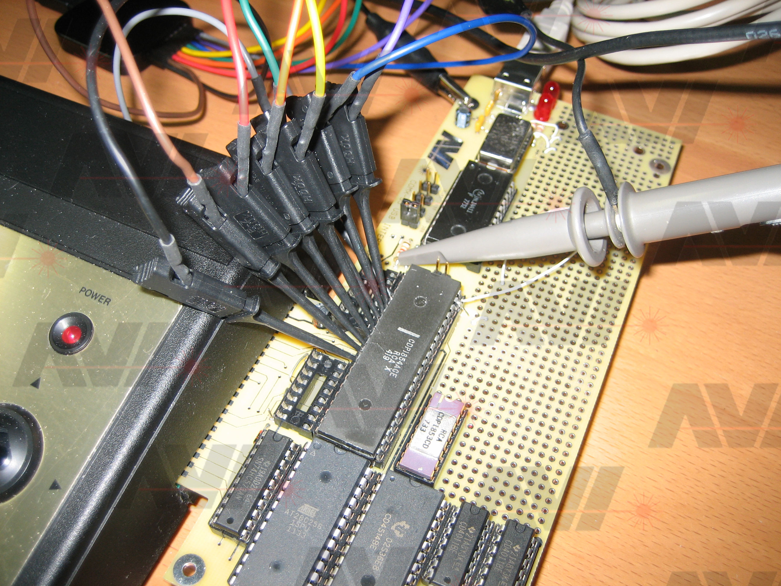
While typing "COMX" on the PC, I recorded the line on the UART.
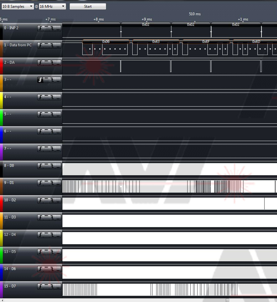
On the second trace line you can see the following values: 0x06, 0x43, 0x4F, 0x4D. Which is great, except for the 0x06, I don't know where that is coming from. The other three characters are 'C', 'O', 'M'.
I used the markers in the logic analyzer software, and see some junk on the data bus right after the INP2 (first trace).
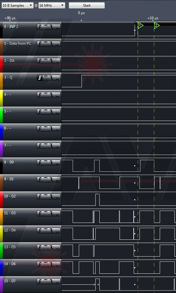
There is always an extra byte before every receive. After some more testing and a few firmware updates, we determined that the UART needs to be flushed before all receives. This was not a problem because Marcel and I decided that all communications would be initiated by the COMX. This makes the PC a giant accessory to the COMX.
Last week of Sept
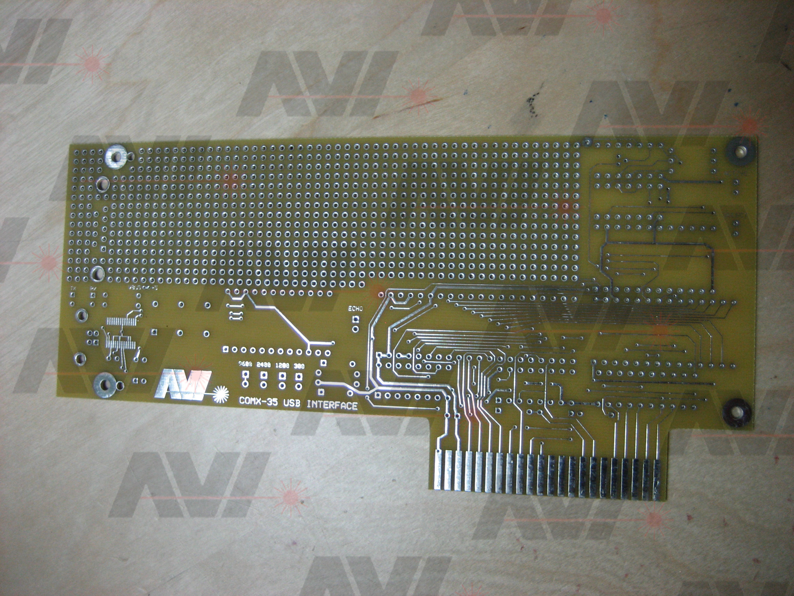
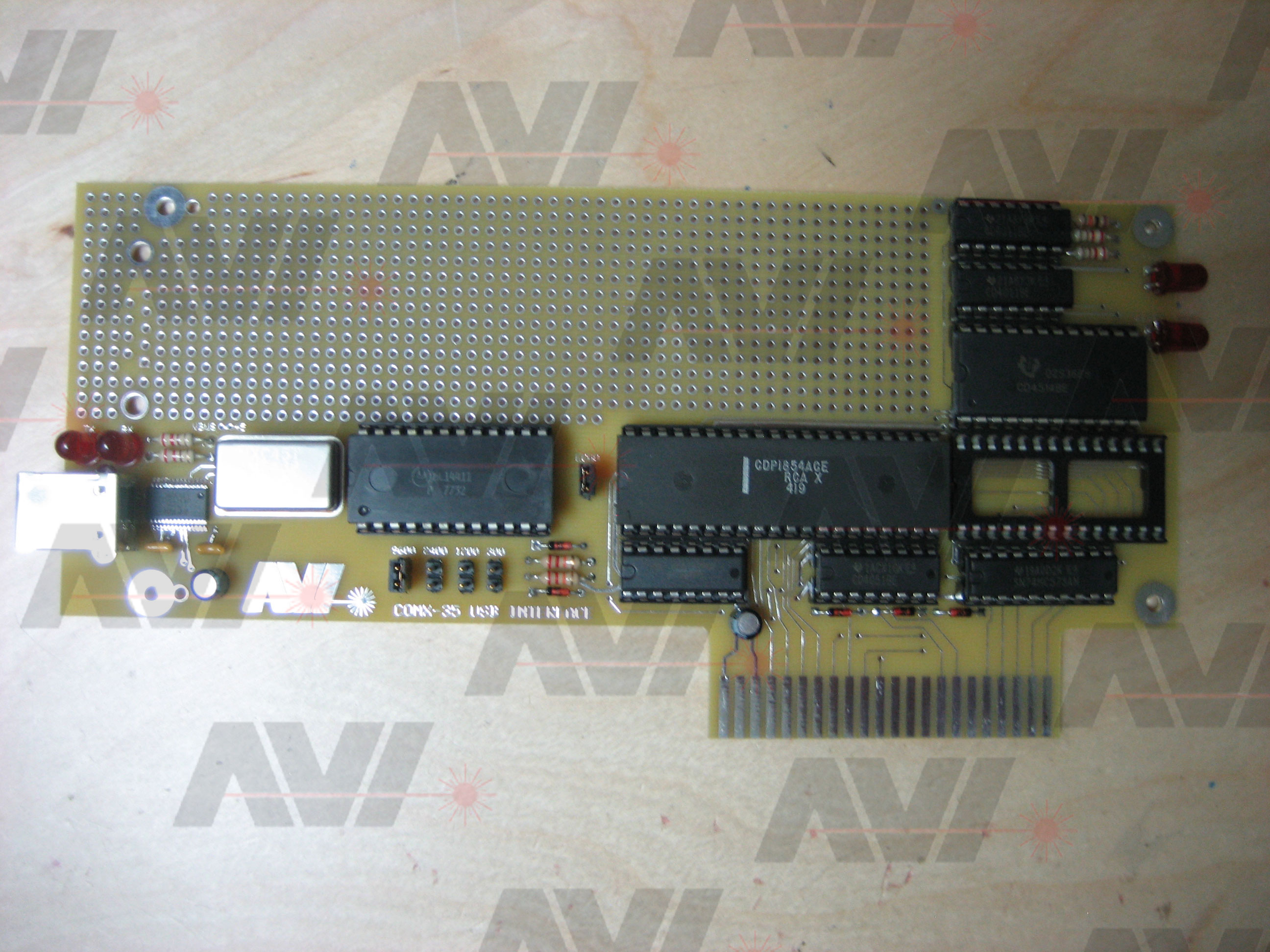
I updated the USB card circuit so it was wired to handle both TX and RX at the same time. It's a mess, but it works. I built a second board and sent it to Marcel. Here are a couple pictures of the board.
At this point I took a break from the USB card hardware. Marcel kept working on the firmware. I tested each version of the firmware as he made it available. We used Drop Box to transfer information.
As Marcel coded, I turned my attention to researching the COMX-35 itself.
COMX <-> PC COMMUNICATION
Marcel had written a lot of the USB card firmware and had it running quite well. We now needed some software on the PC side. I sent Marcel a little USB device to help with testing. I wrote a simple Visual Basic example of how I do serial communication on a PC. Marcel had the COMX talking to the PC using his software in no time.
We worked together, mostly Marcel (I just made suggestions), to get a handle on the types of information that would need to be transferred. I suggested using some sort of header. Marcel came up with a header format that would allow us to do pretty much anything we needed regarding interfacing with the PC.
Ed's idea to use some kind of header with all file information was great. This structured my design quite well. The format we decided on at the start has worked very well. Apart from adding bytes it has stayed more or less the same as when we started out. The header contains the command type requested by the COMX, filename as well as details about the type and size of the file.
Before every action requested by the COMX a header is transferred from the COMX to the PC and one back from the PC to the COMX with the result. For most commands both headers are 64 bytes in size except for commands like USB CAT and USB CD in which the return header is 128 bytes to transfer more information in one go.
If you would like to see how the headers are formatted, you can download this file:
Header FormatSUPER BOARD (Rev1)
First week of Sept
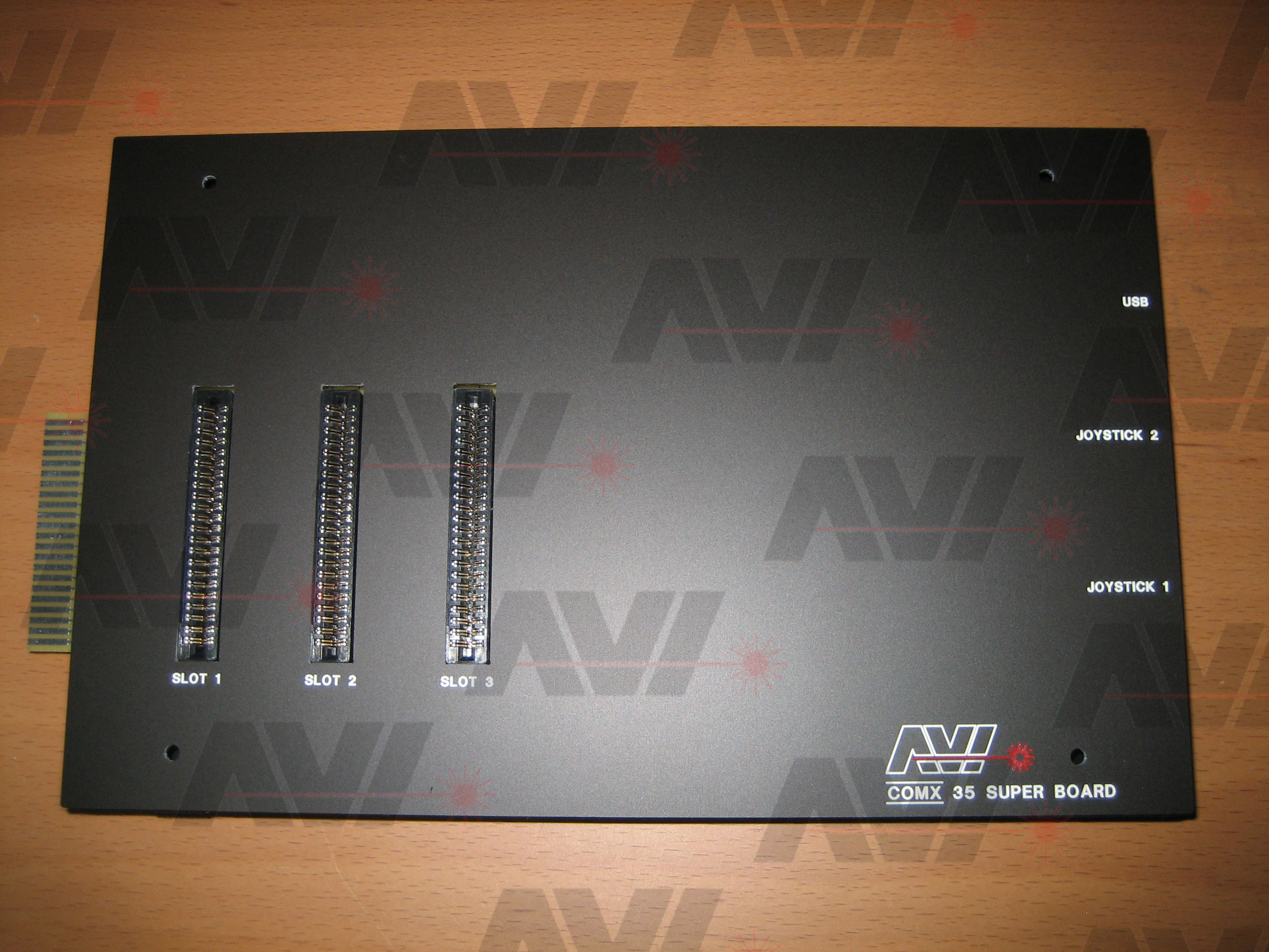
Having the USB card working the way we wanted, it was time for me to start laying out a PCB for it incorporating all the fixes I had made to the previous board. As I started placing components, it became obvious that I would have a bit of extra space on the PCB. I asked Marcel if there was anything else we could add to the card that would add value and make use of the space. We tossed around a few ideas. I drew up this based on our conversations:
When Marcel saw this, he said "I think that would give us a super board!". The name stuck.
Rather than jump right into hardware design, Marcel and I started thinking through what the board should do and how the memory should be mapped out. We worked out the features the Super Board should have. I am going to condense a lot of time here and list what we came up with.
- The Super Board would have:
- - A system ROM that replaces the internal COMX ROM.
- - Two 32K EEPROM chips that would be mapped into the C000h-DFFFh range. These were to be used like the "F&M EPROM Switchboard". (http://www.emma02.hobby-site.com/comx_eprom.htm)
- - Two 32K RAM chips that would be mapped into the C000h-DFFFh range. These would act as if two 32K COMX RAM cards were installed. (http://www.emma02.hobby-site.com/comx_32kram.htm)
- - Two joystick ports. These were to give the Super Board "F&M Joy Card" capabilities. (http://www.emma02.hobby-site.com/comx_joy.htm)
- - A USB interface to connect to a PC.
- - A real time clock.
- - Non-Volatile RAM to store Super Board configuration.
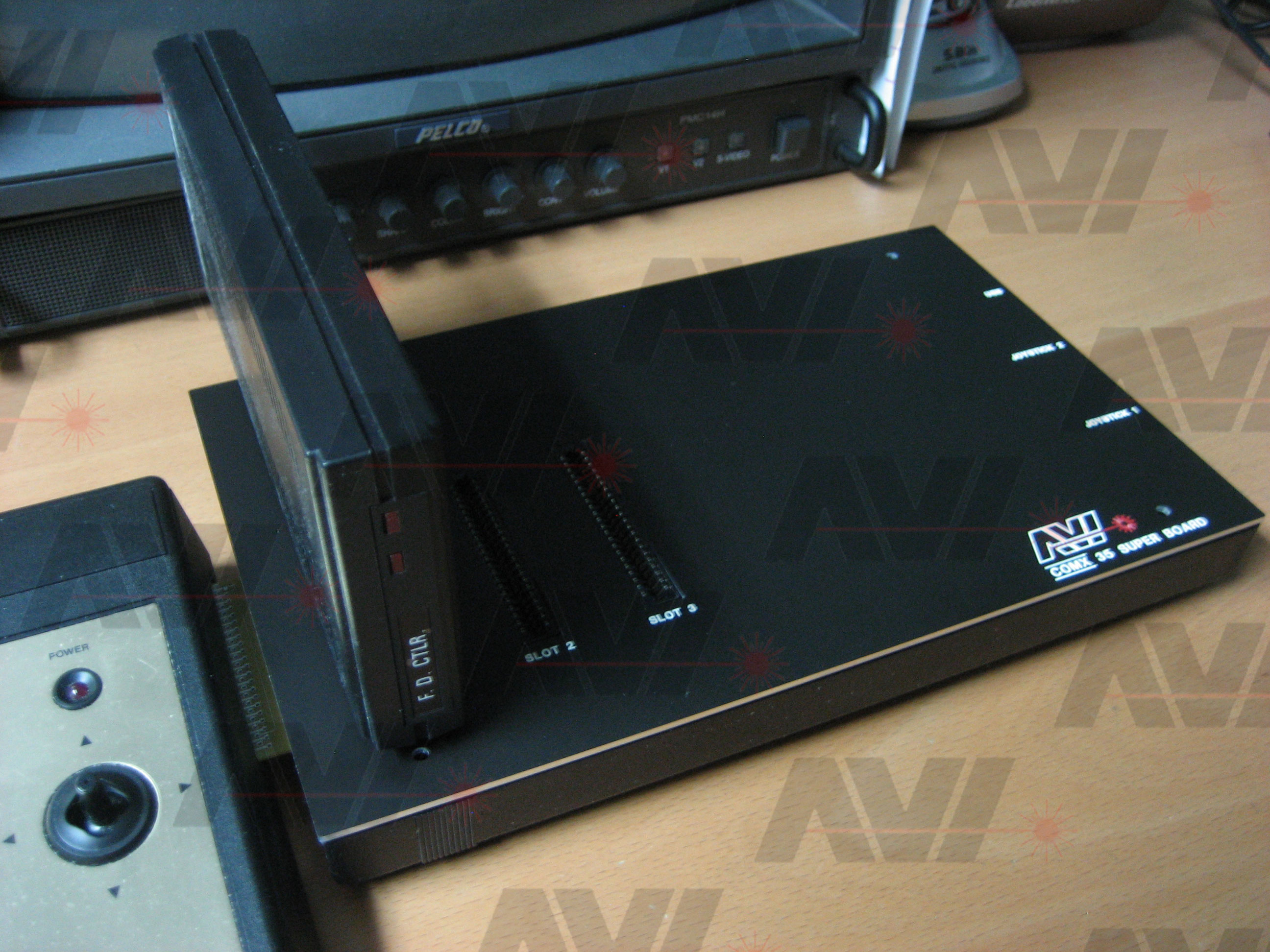
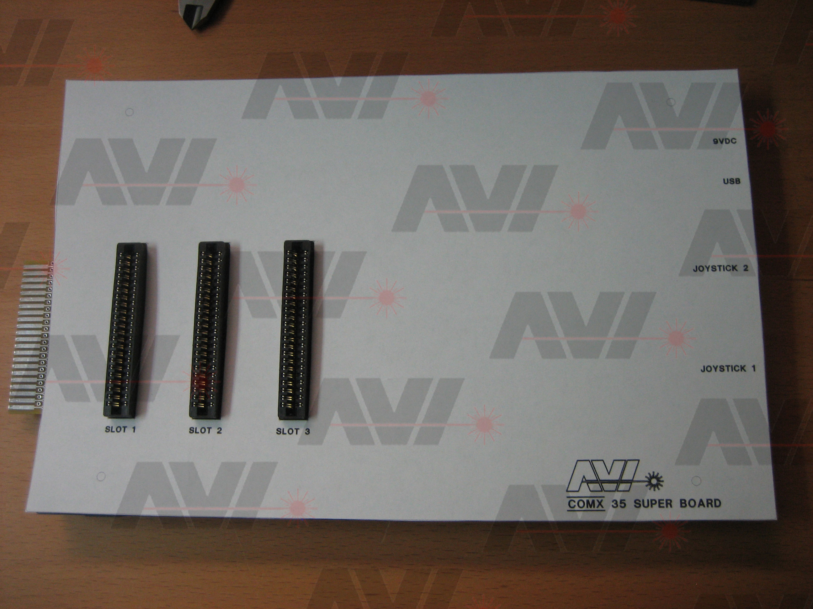
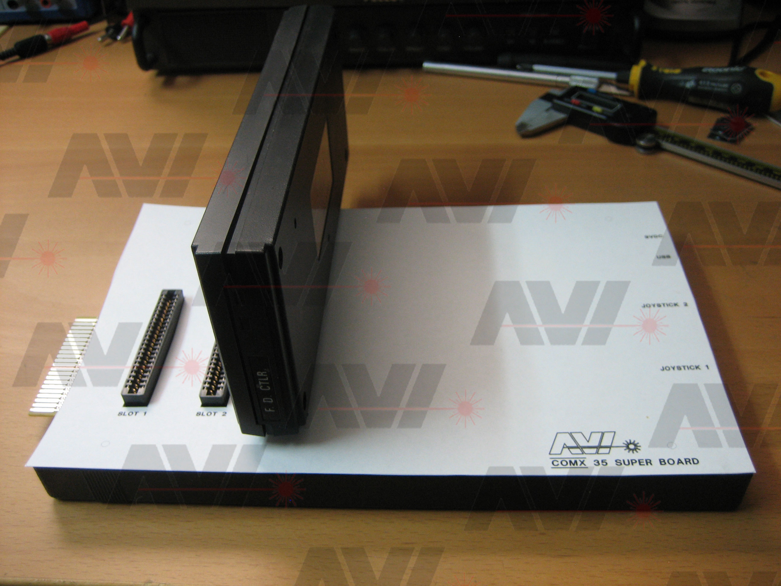
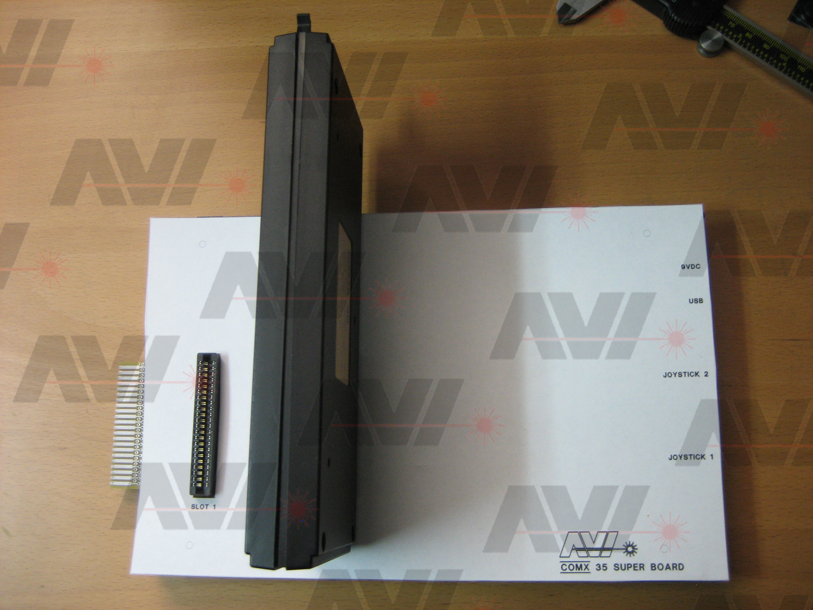
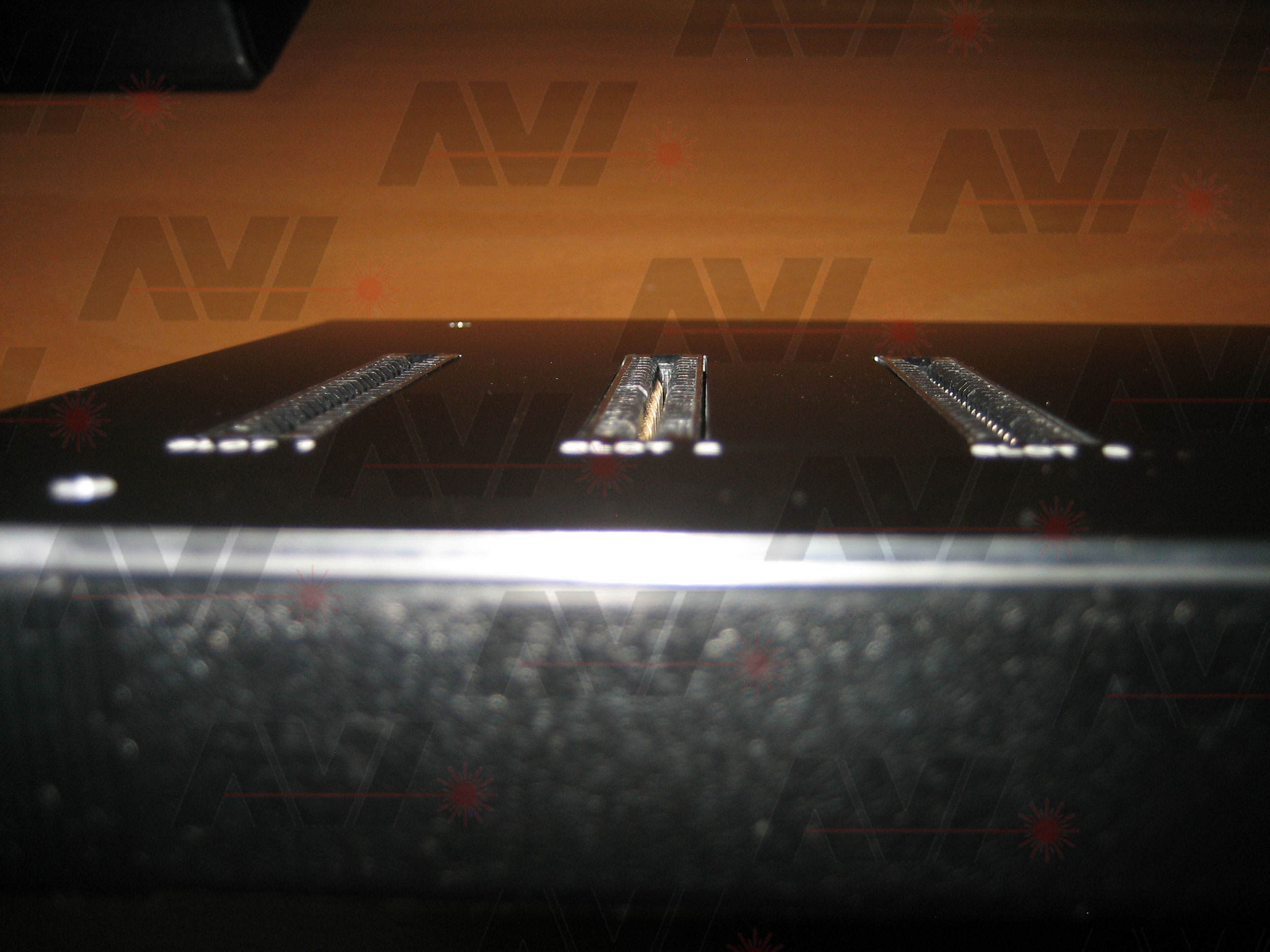
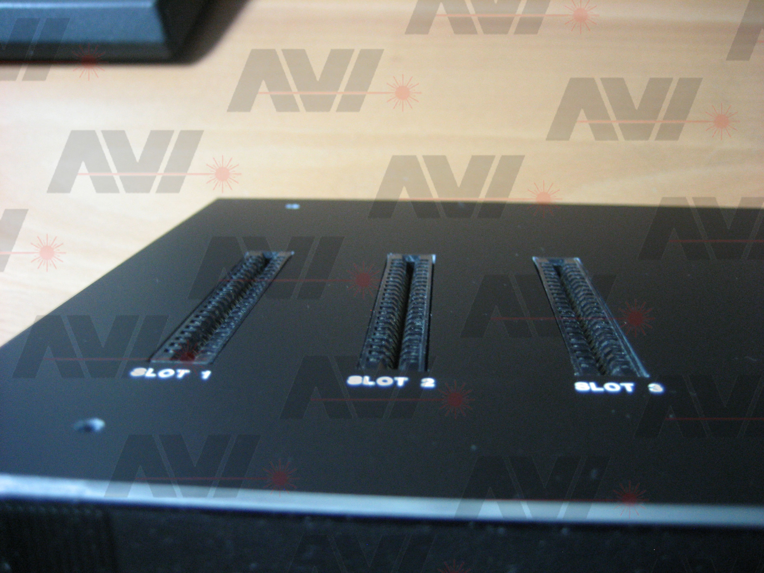
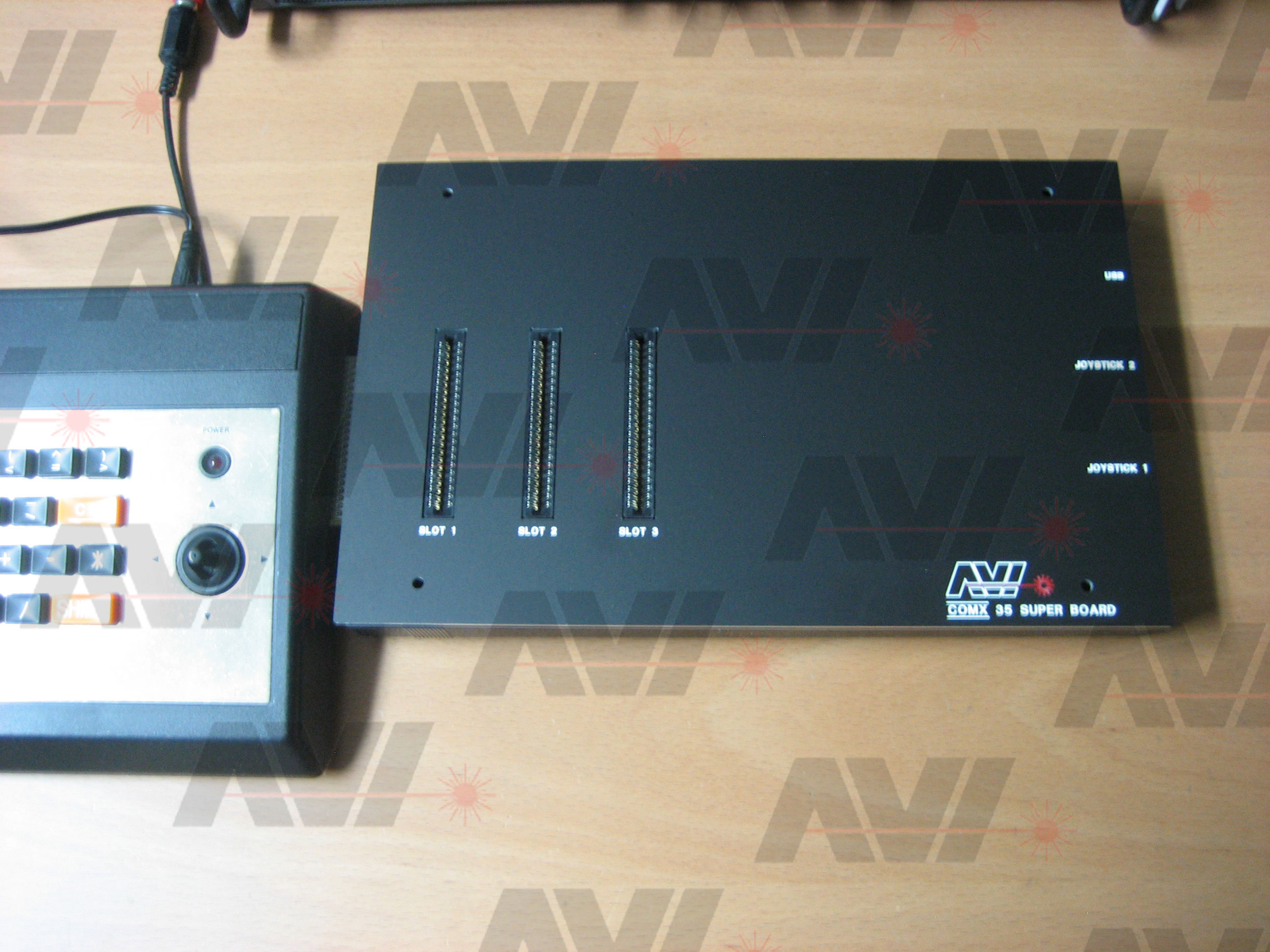
- - Three expansion slots to allow use of existing interface cards. This would replace the need for a COMX expansion box. "Slot 4" would be reserved for the Super Board. (http://www.emma02.hobby-site.com/comx_expansion.htm)
The Super Board hardware allowed for so many more features in the firmware.
First the COMX ROM replacement allowed fixing the following bugs:
- - Removal of red dot in 'shape' of exclamation mark
- - At COMX boot-up setting the temporary stack to 4FFFh is changed to BDFFh to avoid change of RAM memory locations 4FF7h-4FFFh during boot-up
- - Crash when typing '10 TOUT' on clean startup, TOUT is replaced by USB anyway but still '10 USB' will not cause any crash either.
- - Crash on typing READ x when no DATA statement is available in the loaded BASIC program.
- - Crash when 65535 line number is typed
- - Crash in F&M expansion ROM where CARDS caused a crash
Second advantage of the ROM replacement was actually changing things in COMX BASIC, of course adding the 'USB' command but also changing the error code routines to print actual error code text instead of numbers.
Both the Expansion box and Floppy drive controller firmware overwrite some of the internal ROM as well. With the new Super Board internal ROM replacement that was not necessary anymore. This would free up 2 KB in the expansion box memory 'map' from E000h to E7FFh. This was very nice to have in the firmware development as that location is not 'mapped' like the C000h to DFFFh area and as such is always available.
The addition of NVRAM gave options to add system settings like:
- PRESERVED OPTIONS
- - Clock display on / off
- - Boot message (W = WARM START) on / off
- - Selected character set (USB CHAR)
- - 80 Column auto start-up (USB EIGHTYCOL)
- - Logo tune (USB LOGOTUNE)
- - Line editor / screen editor selection
- - JOYLOAD value
- - Time and date format
- - Volume
- - Printer settings
Thanks to the ROM replacement, we were able to allow all settings to be activated on boot-up, like selecting the saved character set and starting the 80 column card automatically!
To do all these changes I first adapted Emma 02 to emulate the new Super Board. This allowed me to start working on it while Ed was still designing the hardware. In the end it did take me months even after I had a real Super Board working before I got anywhere close to finalizing the Super Board firmware.
We started with a proposed memory map of:
We had not figured out where to place the Real Time Clock(RTC) and Non-Volatile RAM (NVRAM) in memory just yet.
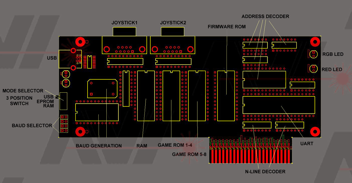
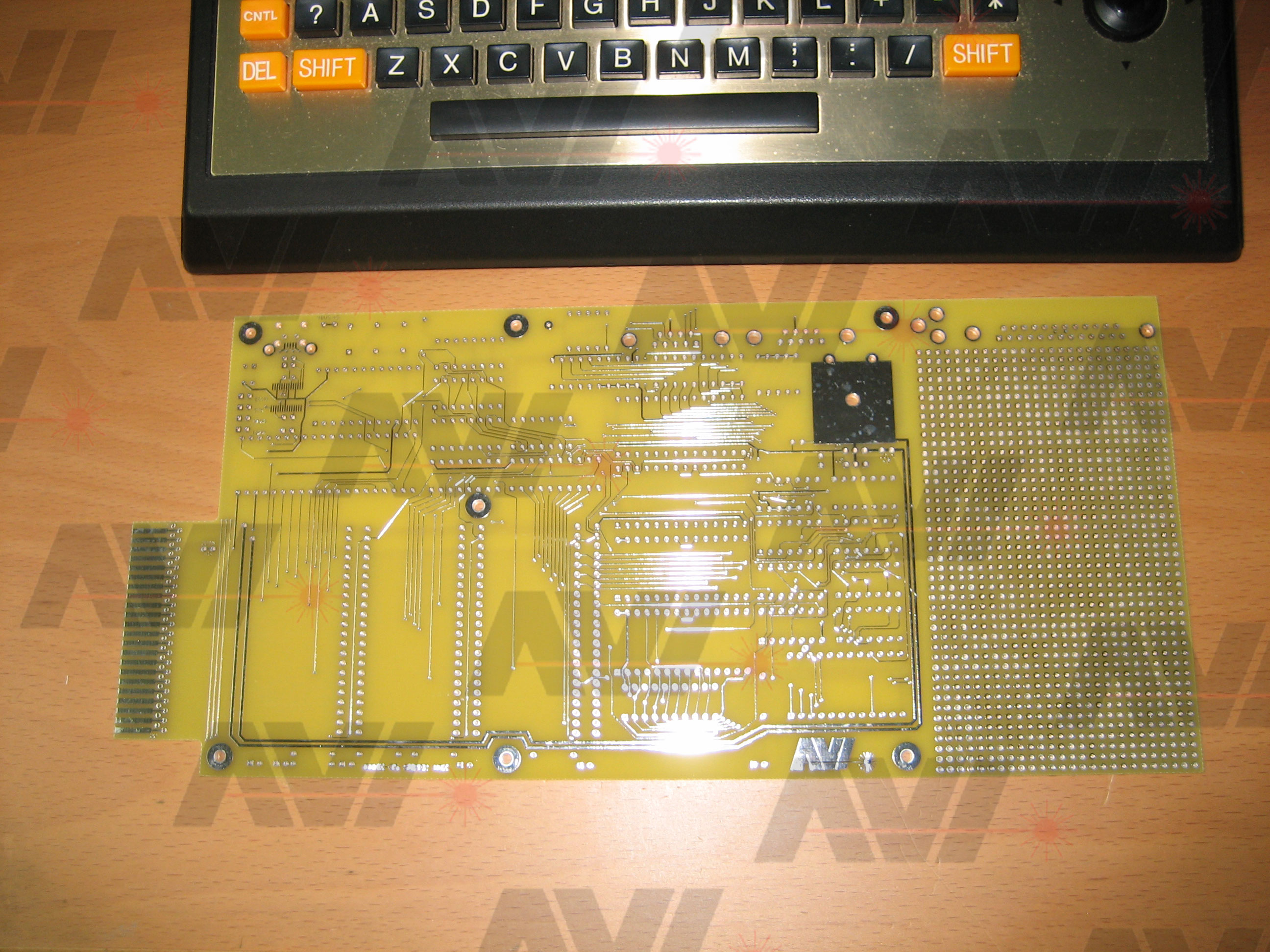
I started laying out the PCB for the Super Board. Here are some mockups of what I was thinking:
Second week of Sept
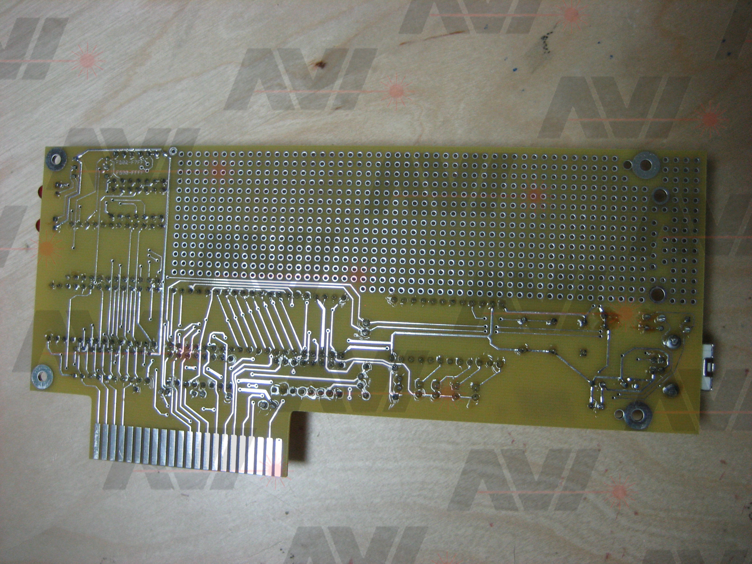
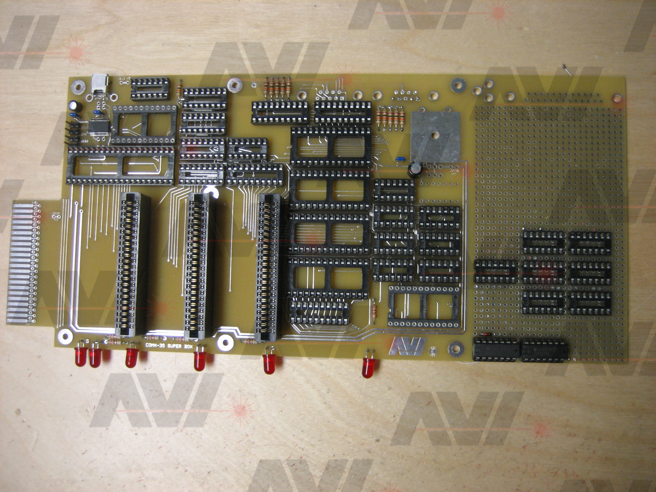
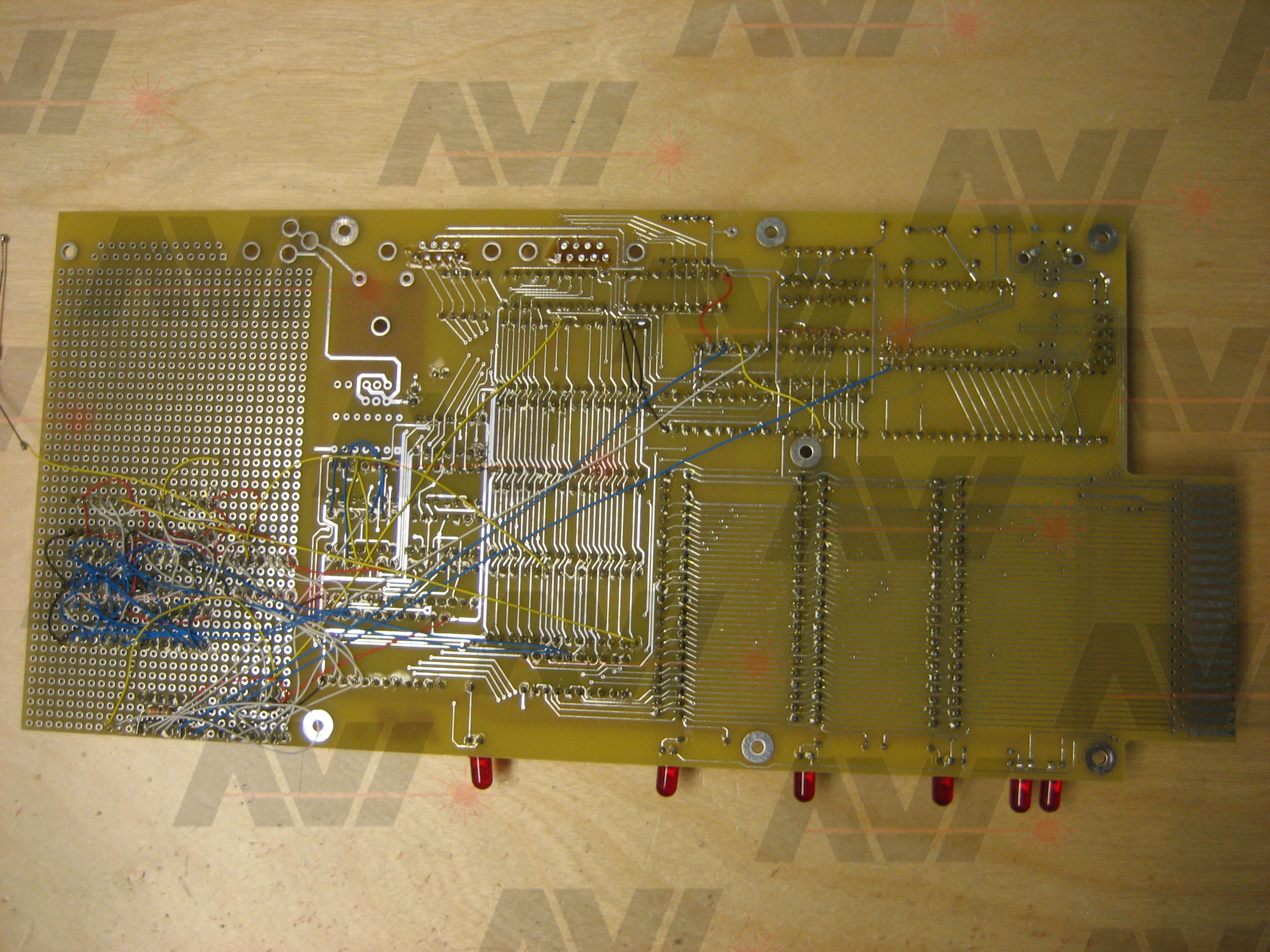
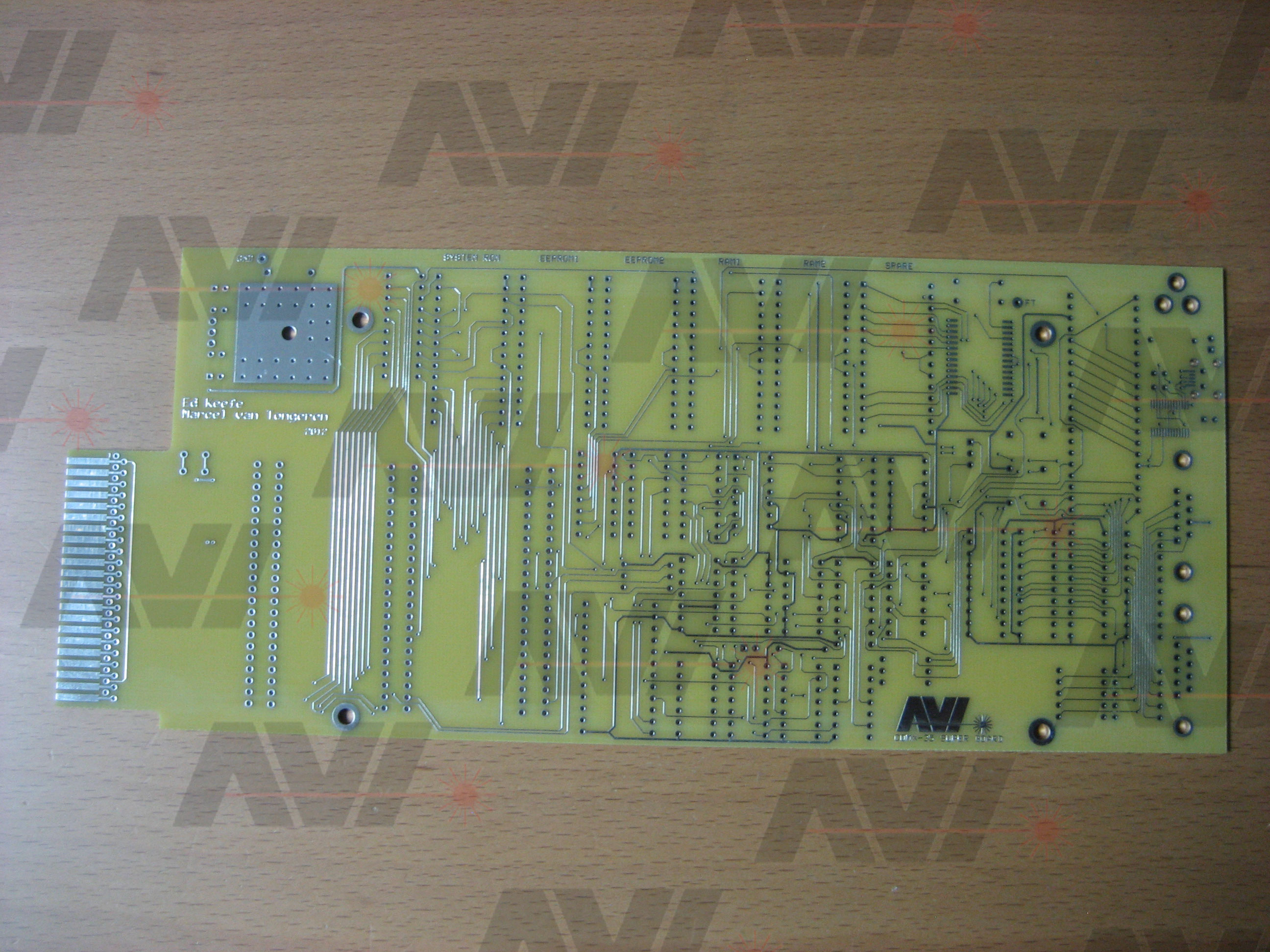
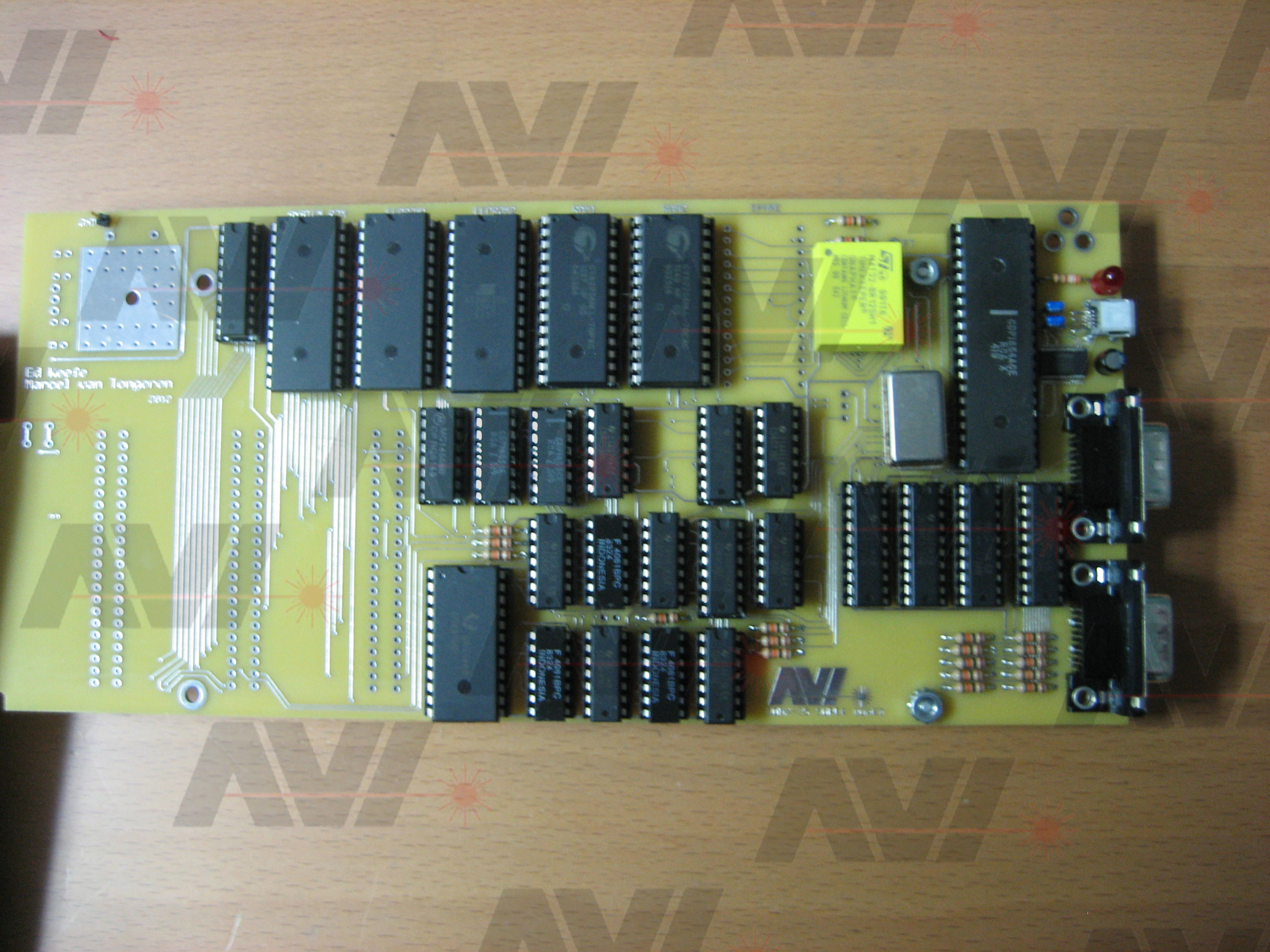
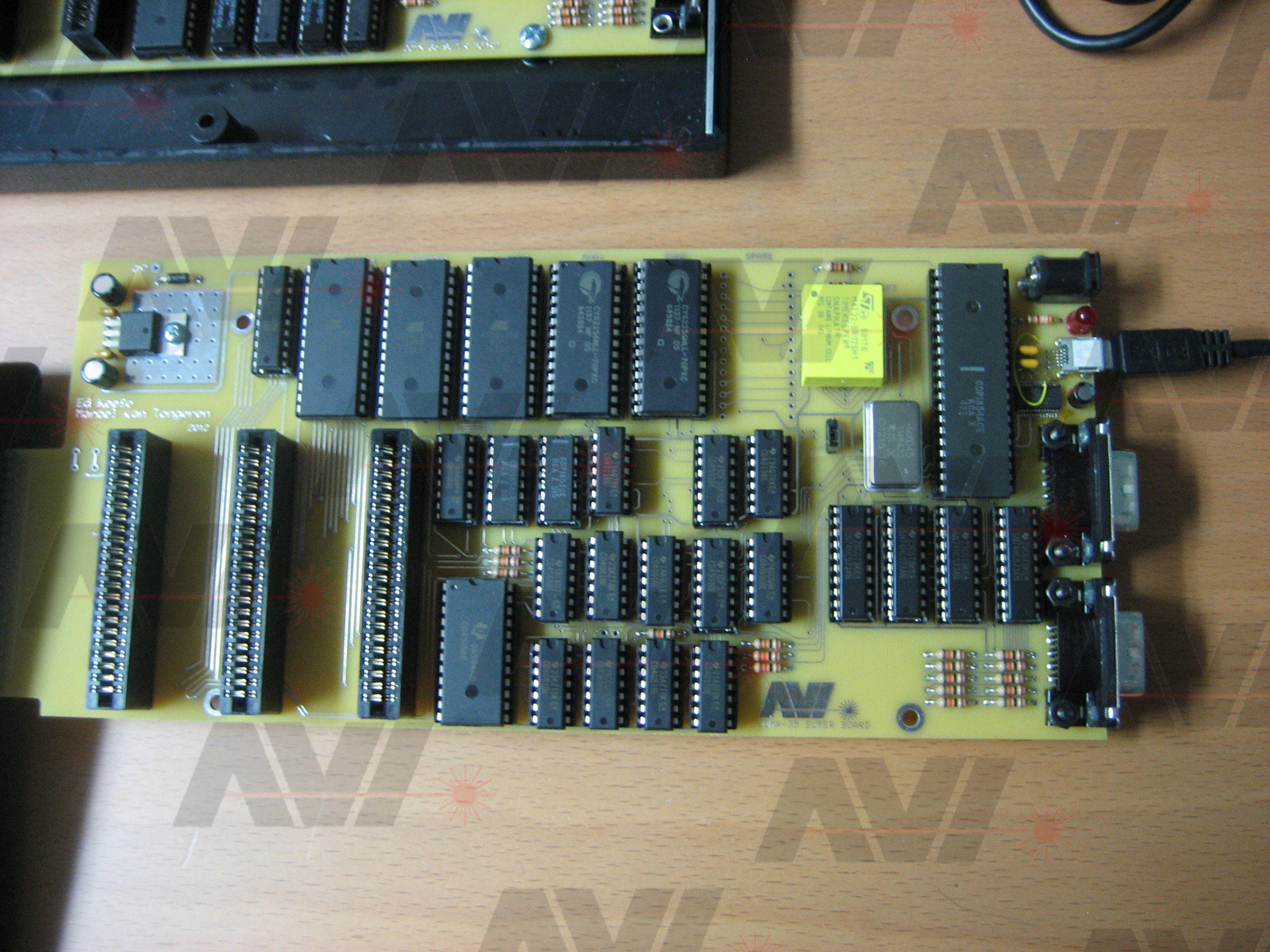
After making sure the mechanical layout would work, I laid out traces. Here is the board I put together:
Bare:
Built:
I was excited to start testing it. I installed all the ICs (which turned out to be a bad idea), plugged it into the COMX's expansion port and powered it up. Nothing! The COMX would not start.
I reviewed the schematic I drew and realized I had a major error in the address decoder. I proceeded to add more circuitry to modify how the board worked hoping to make the address decoder at least run the external system ROM. Here is what I added:
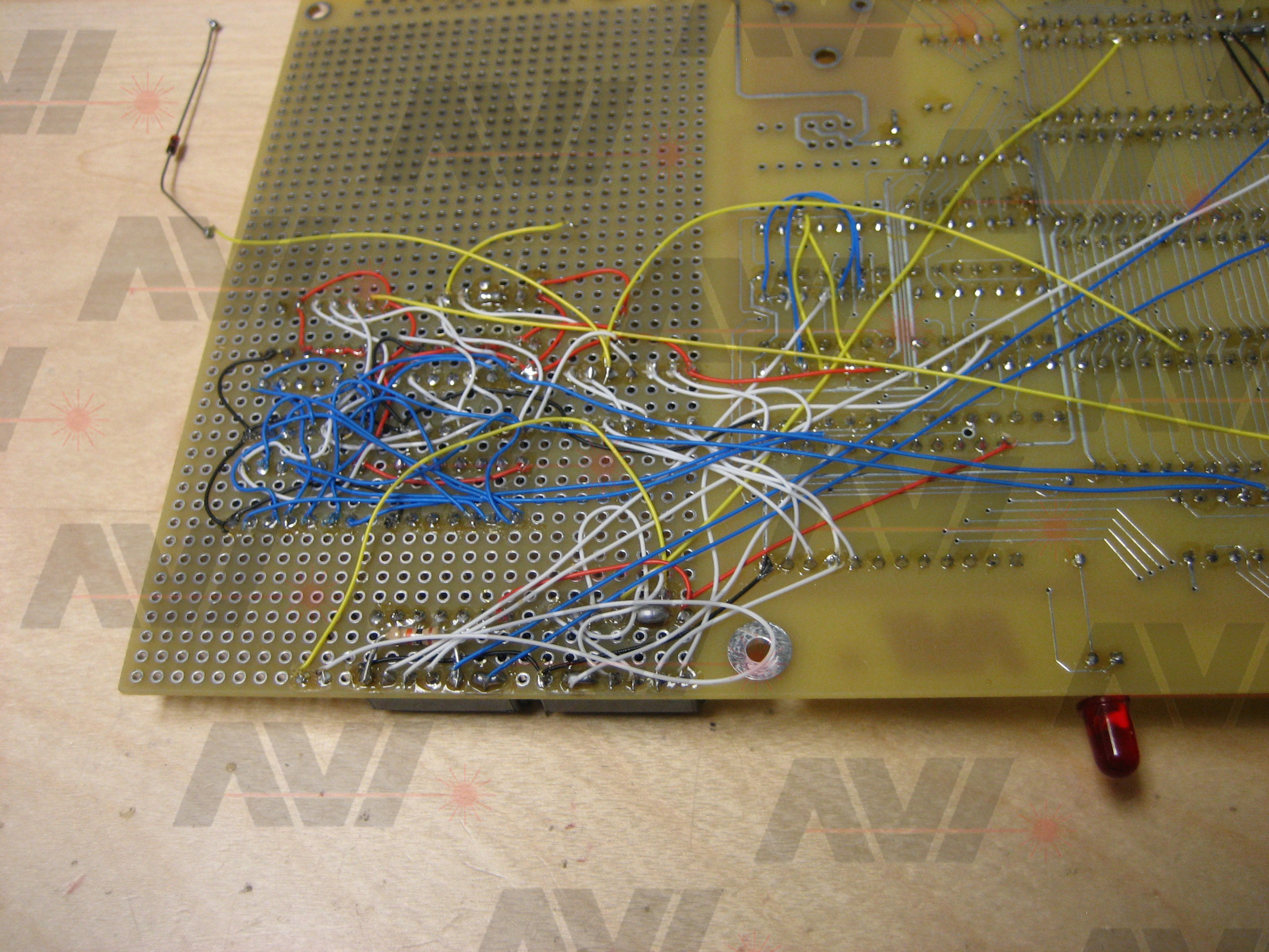
This did not work either so I removed all of the ICs that did not work in the external system ROM circuit. Still nothing. After a lot of testing and head scratching, I decided to start over.
First week of Oct
When I order PCBs, I always order at least two. So I started building the second board, only adding the parts required to get the external ROM running. I built up a single ROM section of the second Super Board PCB.
This time I had better luck. I figured out what was going on. Any time the /EXTROM line (which is on the expansion port to disable the internal ROM) was set low the system would crash or fail to start. If I made it high, the internal ROM would operate and the system would start and run.
In short, I had address lines A13 and A14 to the ROMs under control from the EPROM1/2 and RAM1/2 logic circuit which was not populated on the board yet. So on the second PCB these two lines were floating, causing the EEPROM to act erratically. I wired then to A13 and A14 and the bus started acting as it should. To make matters worse, somehow while I was programming the EEPROM I managed to overwrite the first byte, which should be a C4h 'No-Op', with 00h which is a 'Idle' forcing the system to wait for an interrupt that never came. So even after I had the circuit wired correctly, the system still would not start. I burned the EEPROM with the correct code and the system started up as it should.
At this point I permanently grounded the /EXTROM line to the COMX, disabling the internal ROM anytime the Super Board is plugged into the COMX. Everything worked as it should so far.
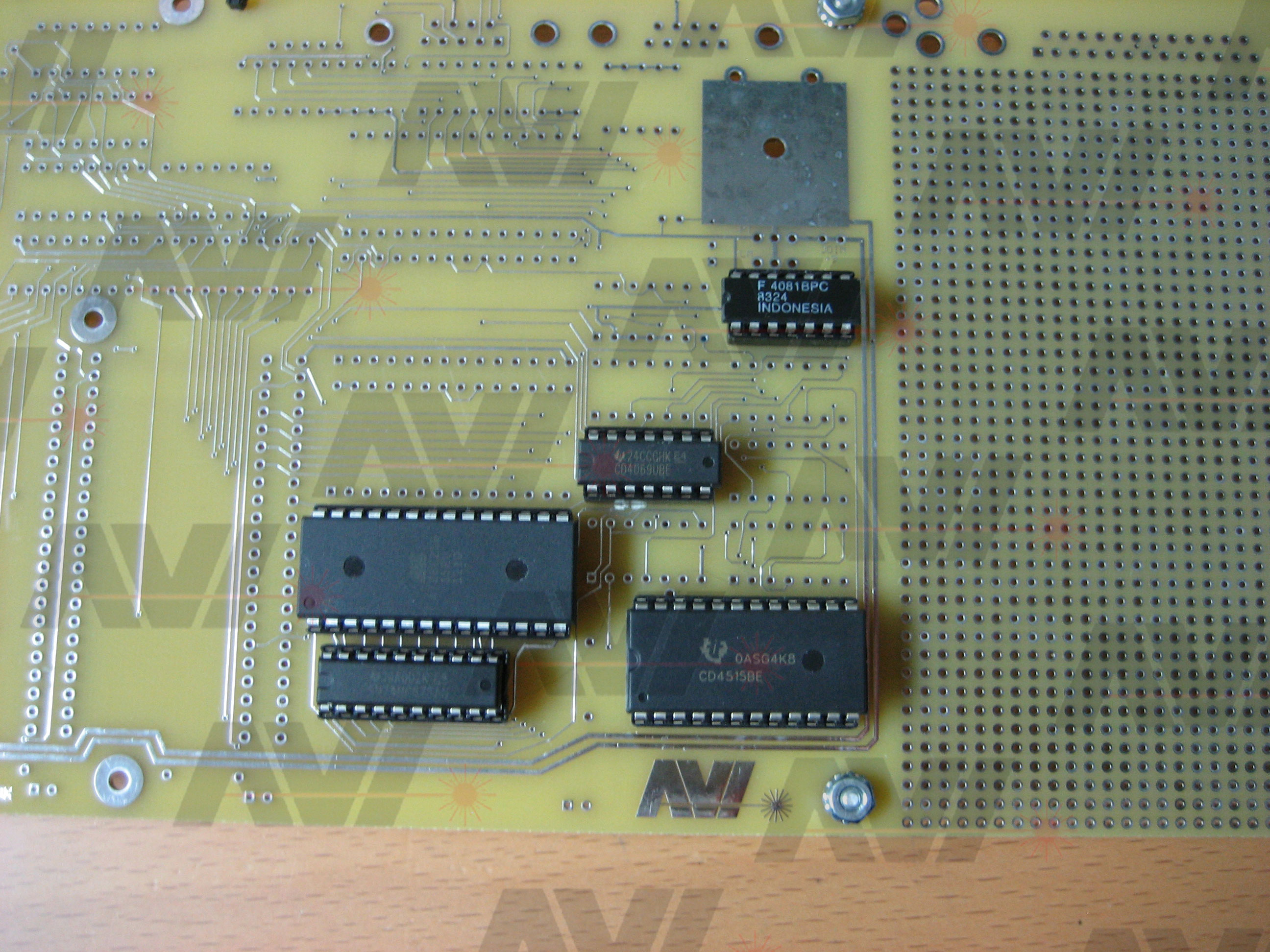
One section at a time, I added the circuitry for the address decoder, N-line decoder and ROM/RAM selection. I tested these additions as I installed them, and they worked as I expected.
With that small success, I then added two RAM chips and the RTC/NVRAM module. The RTC/NVRAM worked as it should but I was having a problem with the RAM. I could select the RAM and it seemed to work fine, but if I mis-typed a command the system would crash.
It turned out to be the way the COMX handles errors. Marcel found that the COMX asserts bit 0 of an OUT1 anytime an error occurs. This was messing with the bank selection circuit. The eight bits of an OUT1 are used to control slot selection, EEPROM/RAM selection and bank switching selection.
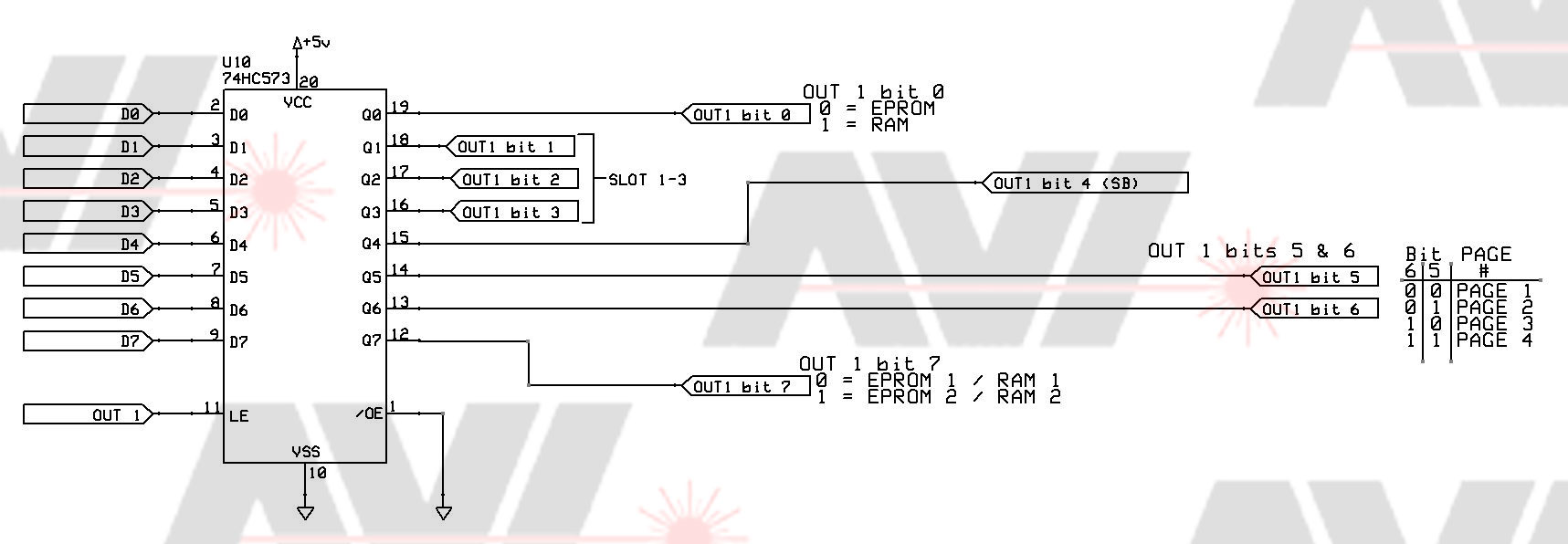
Marcel made an update to the firmware so we now have control over OUT1 bit 0. Bank selection was now working.
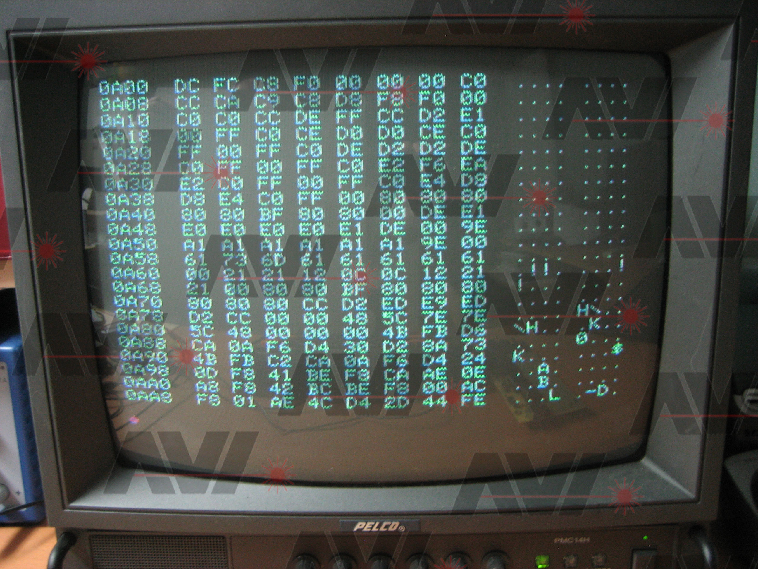
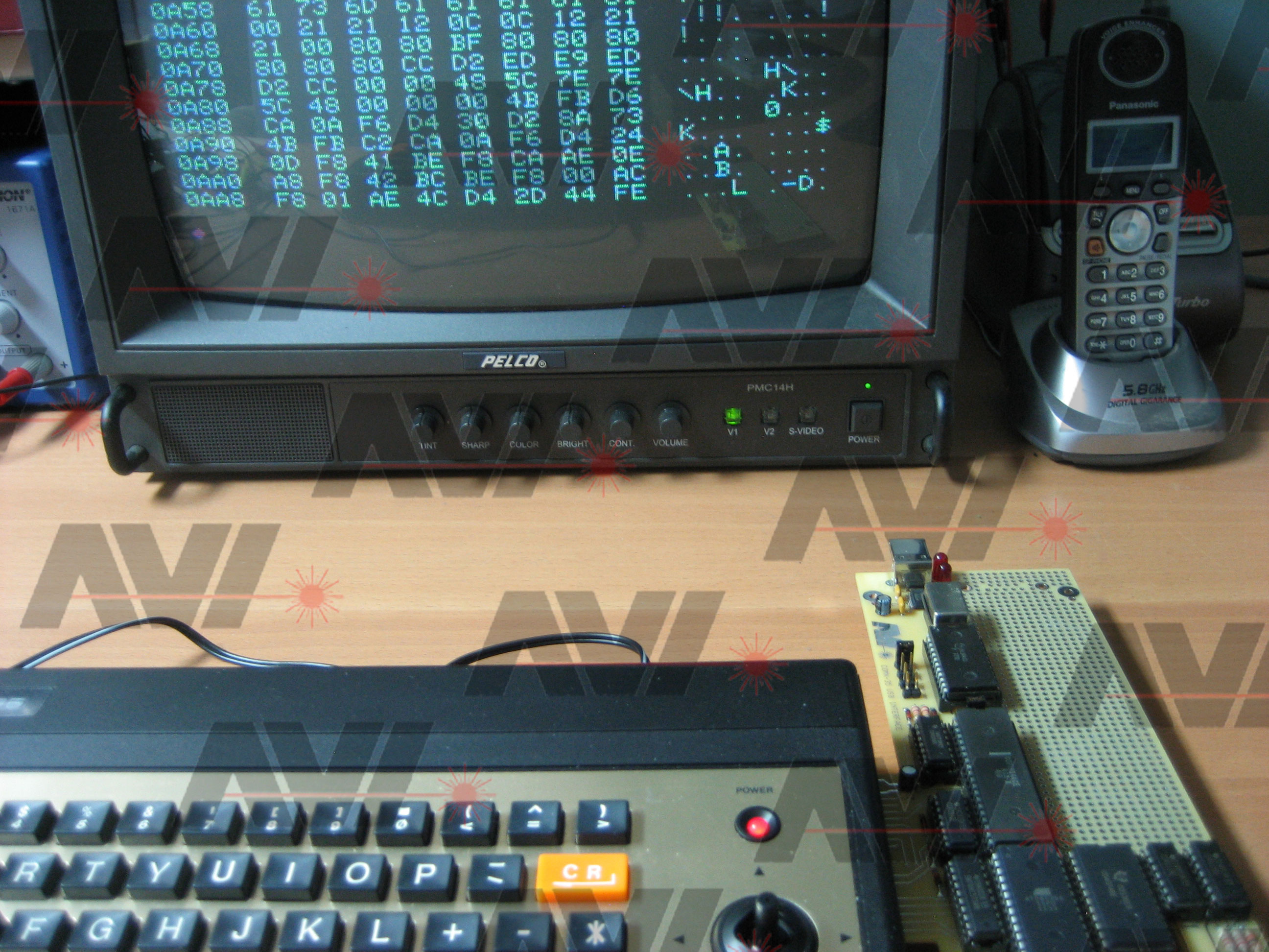
I did some more testing with the EPROM section of the Super Board. I got the board to run a 'USB ROM CAT' with the following results:
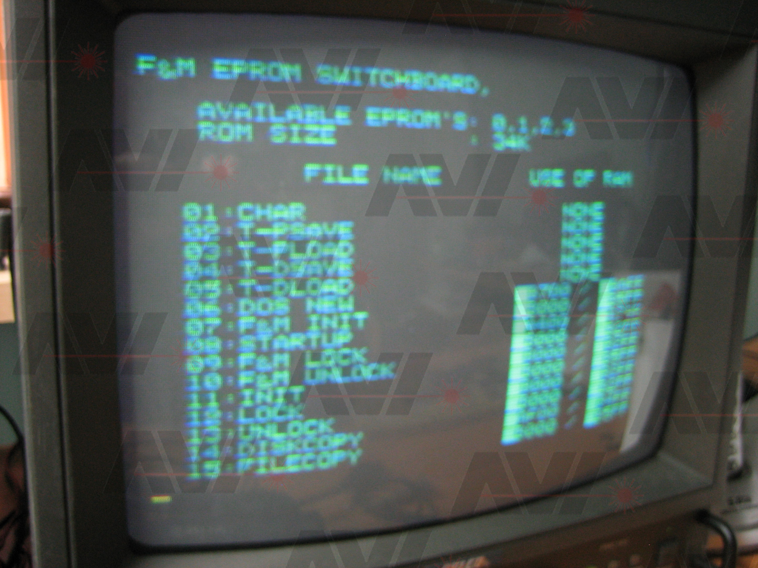
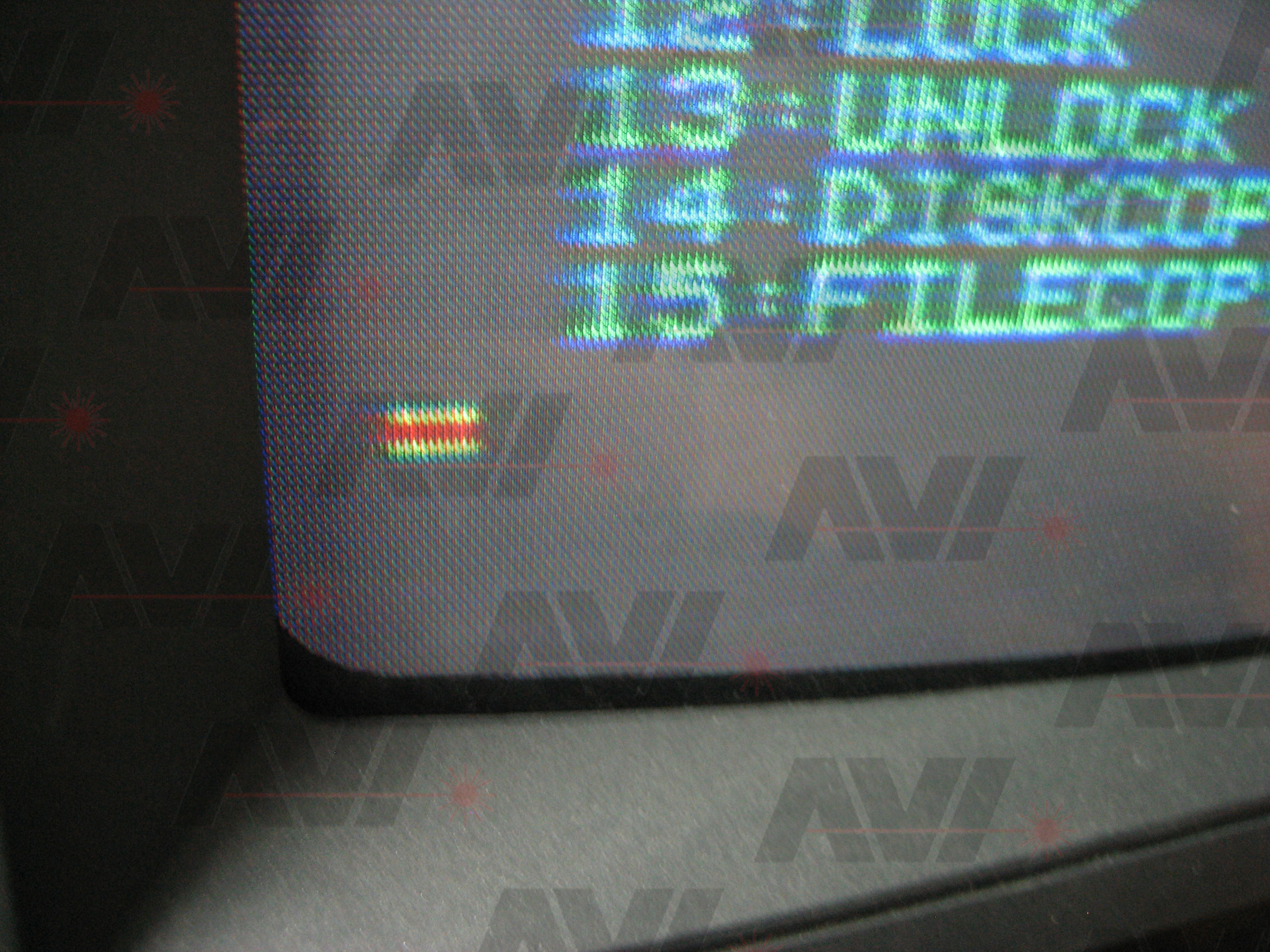
This shows a listing of some of the functions built into the Super Board. However, when I try to do it a second time without a reset or power cycle, it hangs the COMX after '15: FILECOPY ...' with a junk character at the bottom of the screen:
Marcel figured this out and corrected the firmware.
I then added the components for the joy stick interface and tested it. Directional controls worked as they should but the buttons appeared to not work. I had made another mistake. I had INP2 and INP4 reversed. I swapped out the two N-lines and the buttons worked on the correct joysticks.
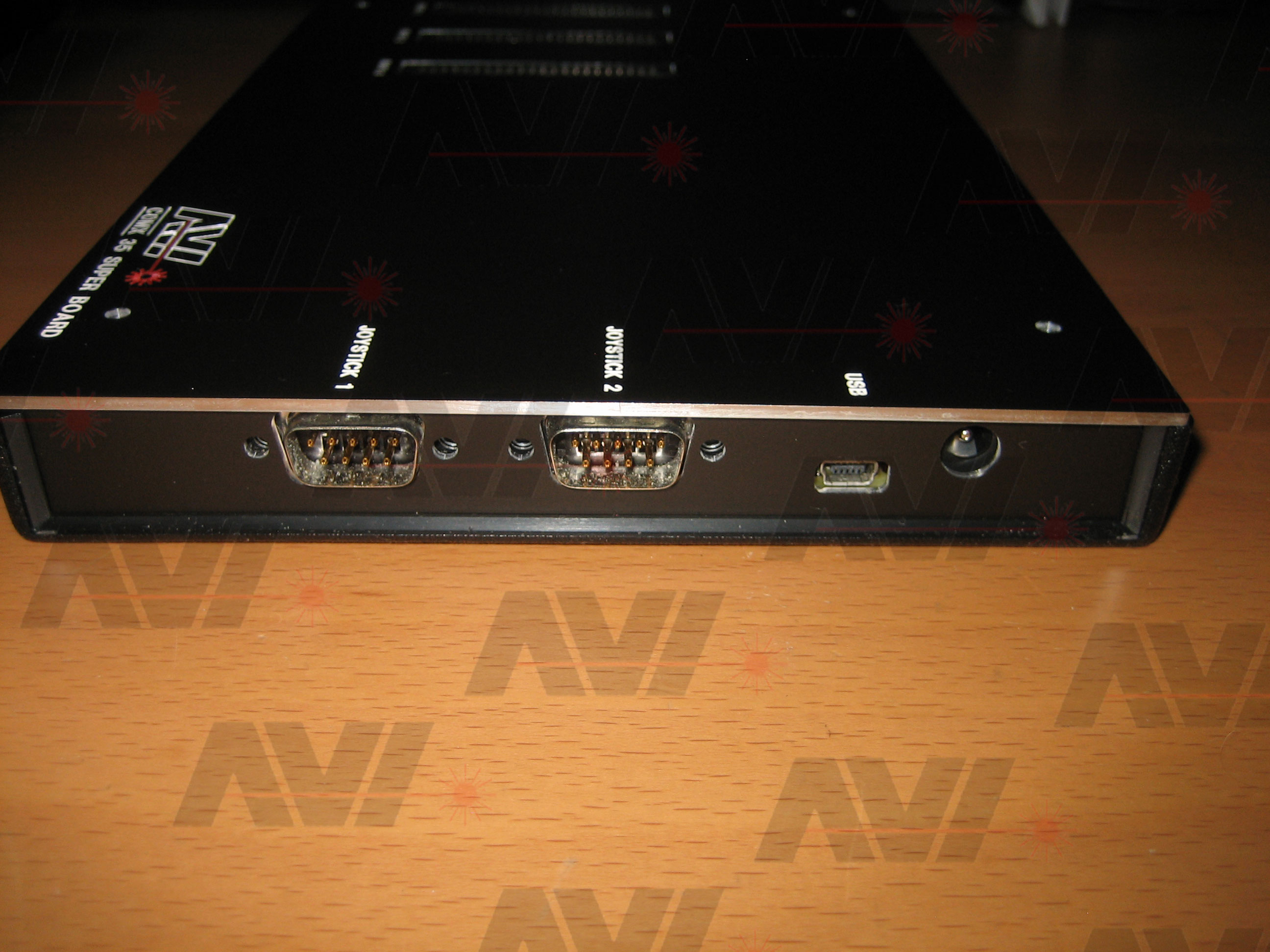
The CDP1854 UART requires a baud rate signal that is 16 times the desired baud rate. The Super Board is designed to use a 1.8432MHz oscillator just like the USB card. 1,843,200Hz divided by 16 is 115,200. 115,200 divided by 2 is 57,600. With this information I decided to no longer use the MC14411 baud rate generator chip on the Super Board. I just wired the oscillator directly to the UART. I added the USB interface chip and tested it. It was fine.
I was able to get the Super Board to talk to the PC at a baud rate of 115,200. I measured a slight speed up, but don't really see it. It should be twice as fast. I will put a jumper on the next PCB that allows selection of either 57600 or 115200 as the baud rate.
The only thing left was to put some sort of write protect in place for the NVRAM. I did this by adding a circuit that responds to an INP1 signal, flipping a 4013 flip-flop to control the /WE line of the RTC/NVRAM module. This signal is also used to latch an 8-bit latch that holds the current state of the write protect circuit. Only the first bit is used on the latch (bit 0 is NVRAM WP state, Bits 1-7 are held low awaiting assignment).
I had everything working (or so I thought, a sneaky bug with EF4 caused loading anything by tape to not work, details later).
- The following sections are built and working:
- - COMX internal System ROM disabled
- - COMX external System ROM in place and working
- - Two EPROMs (0-7) in C000h-DFFFh range in place and working
- - Two static RAMs (0-7) in C000h-DFFFh range in place and working
- - RTC and NVRAM is in place and working
- - NVRAM is write protected based on INP 1 state (0-Write Enabled, 1 - Write Protected)
- - 8-bit latch on INP 1
- - Joysticks A and B are in place and working
- - USB interface
- - 115,200 baud rate
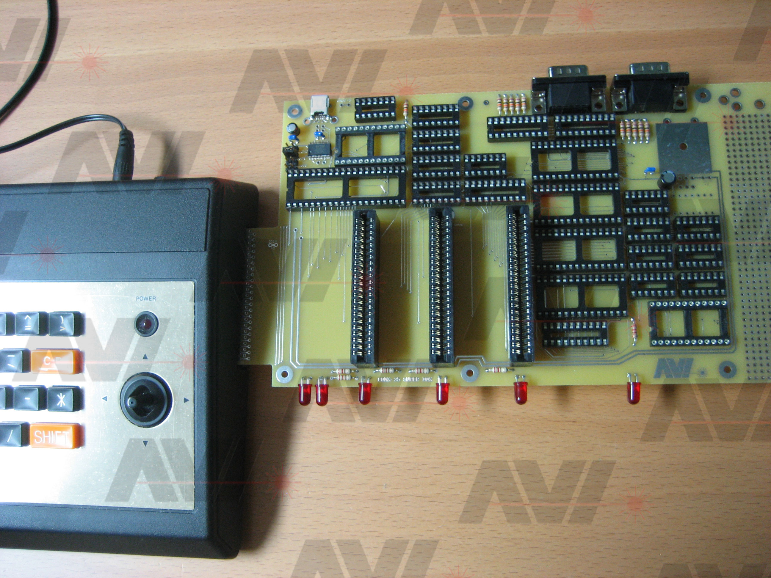
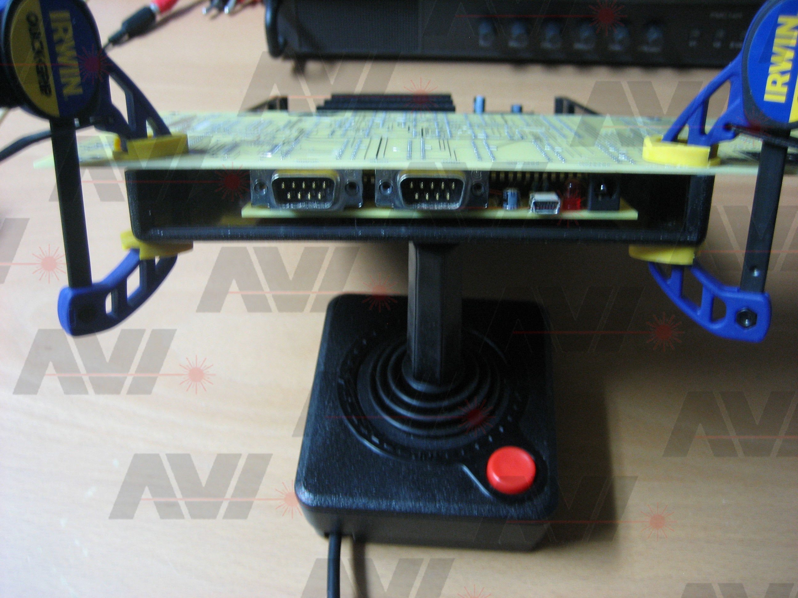
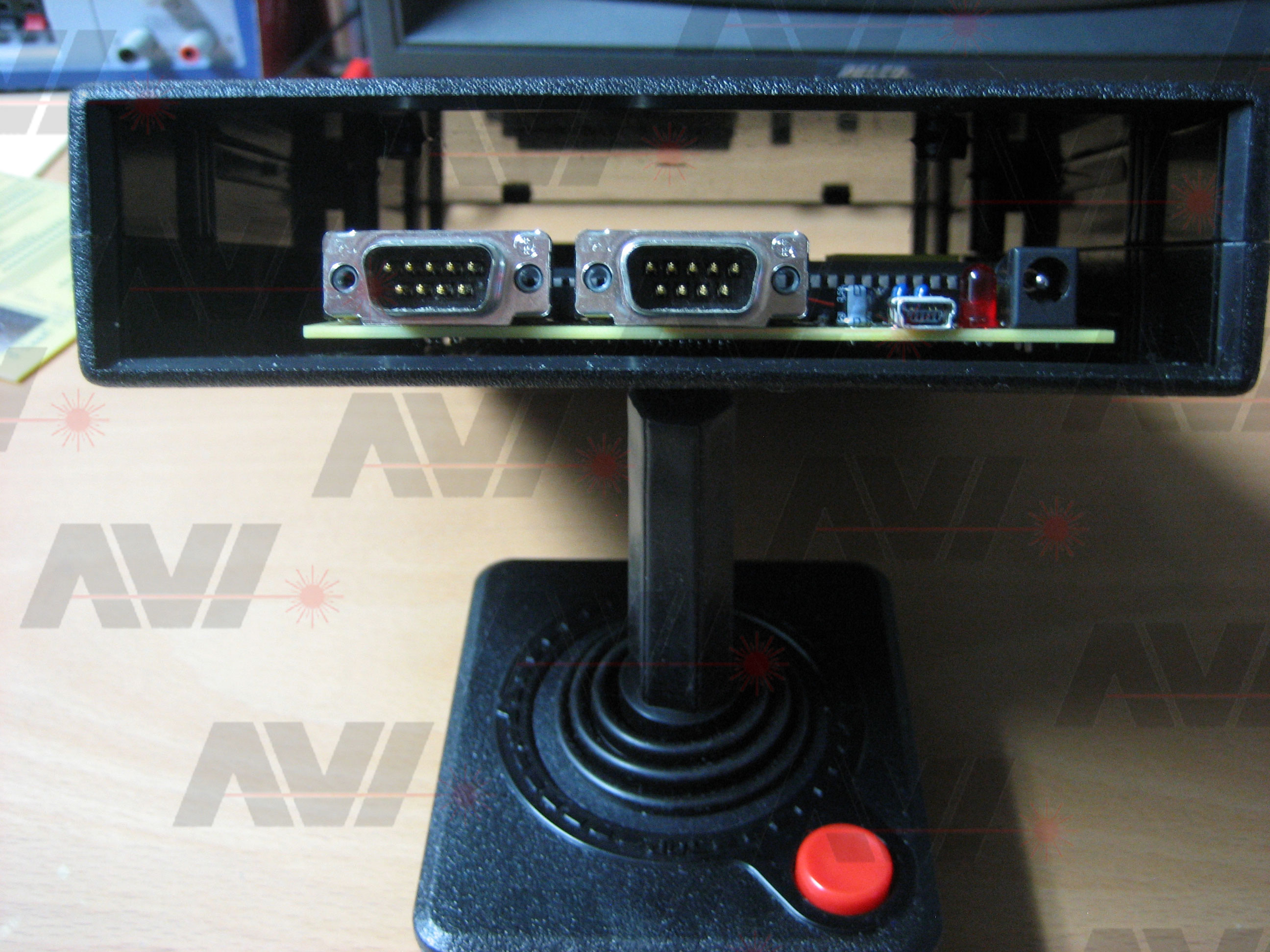
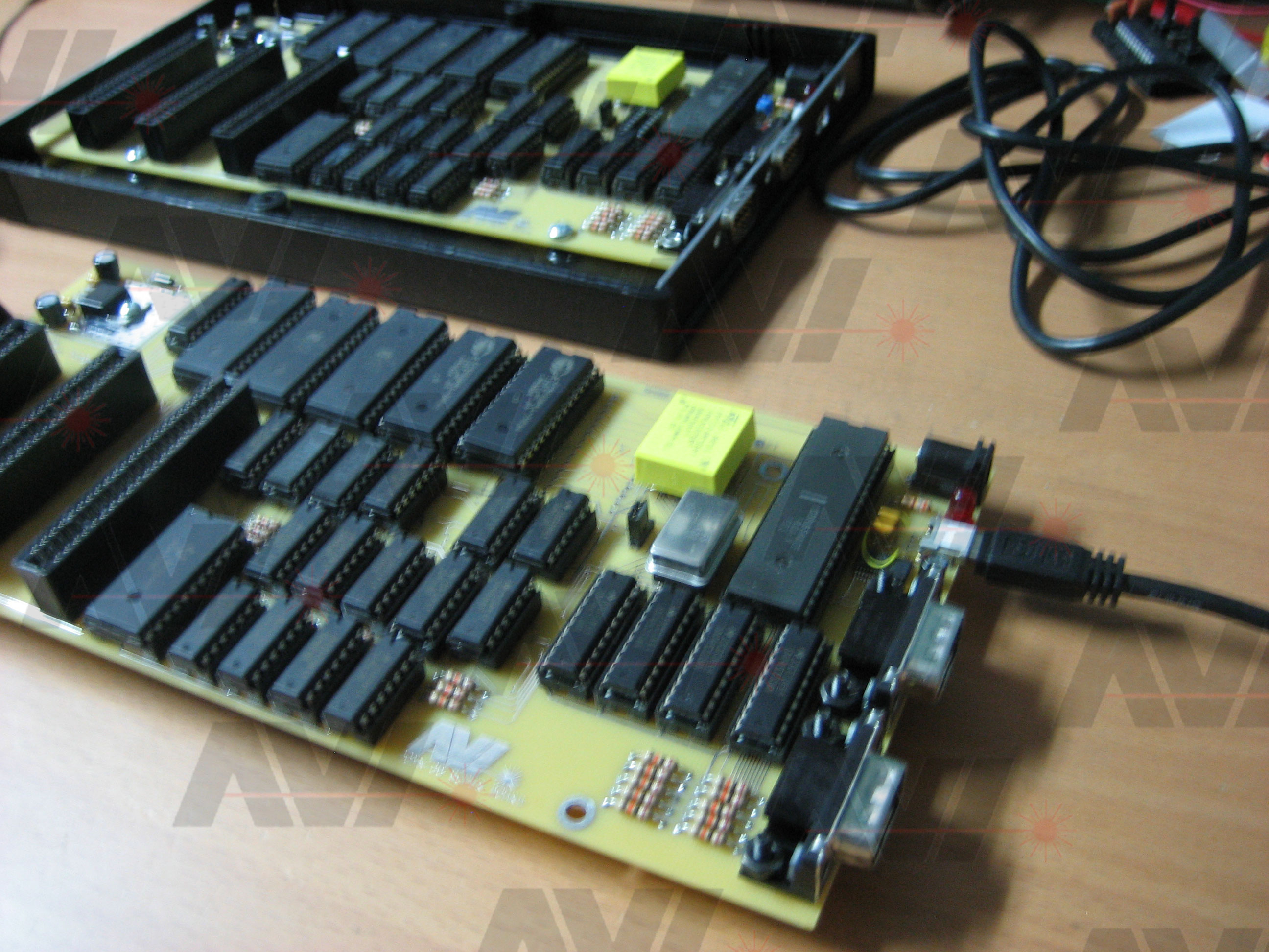
Here is what the second attempt building the Super Board looked like:
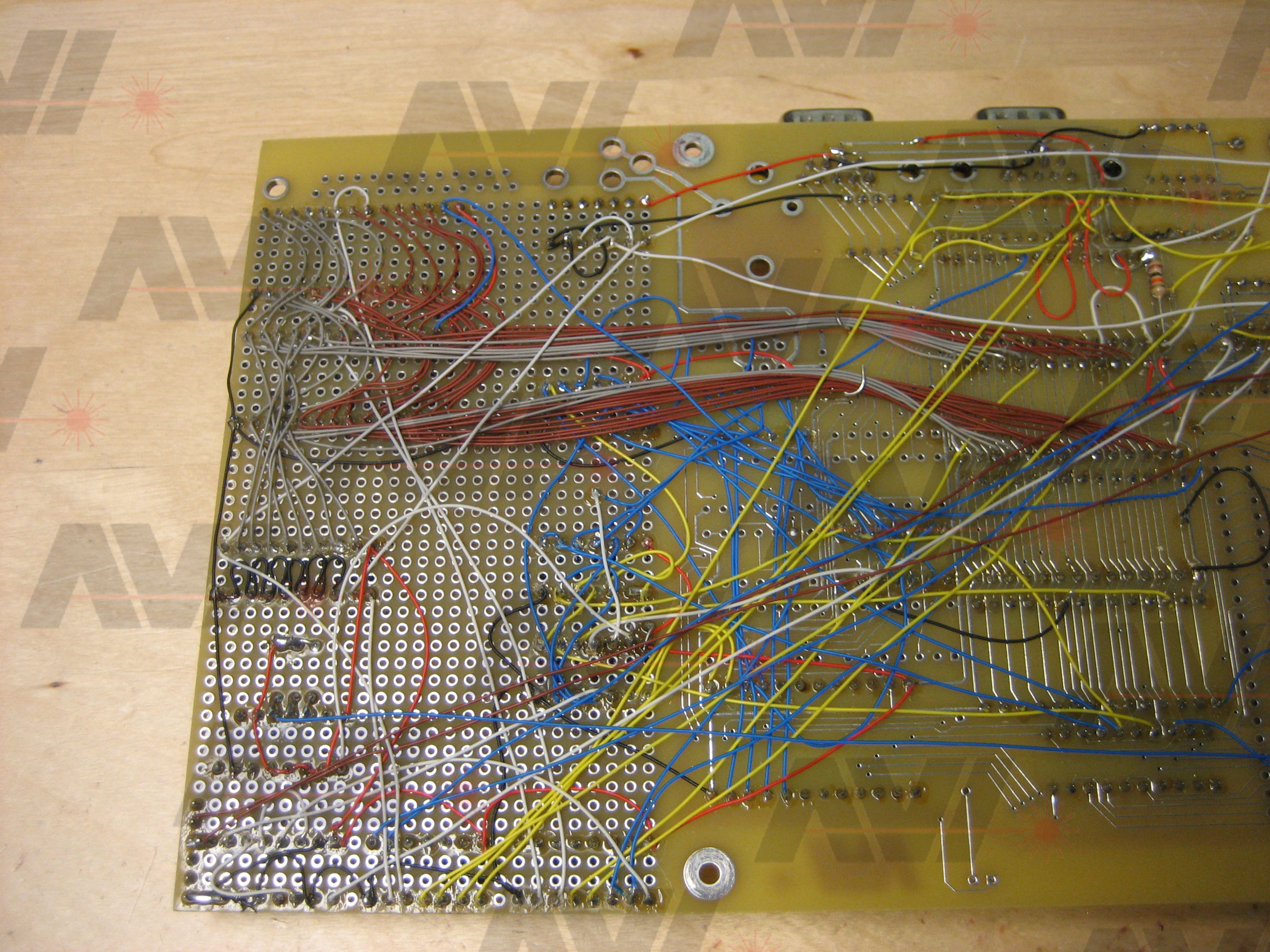
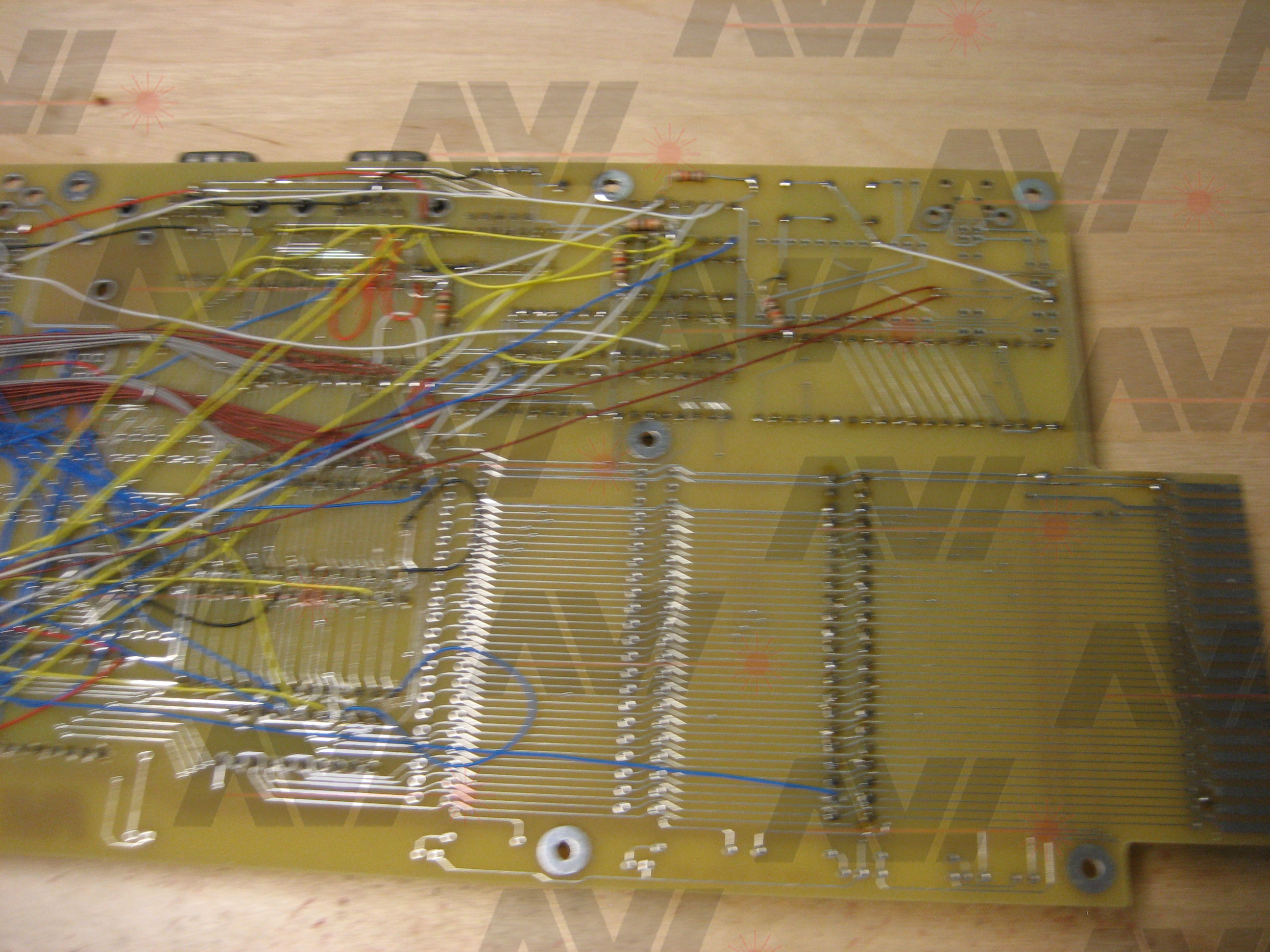
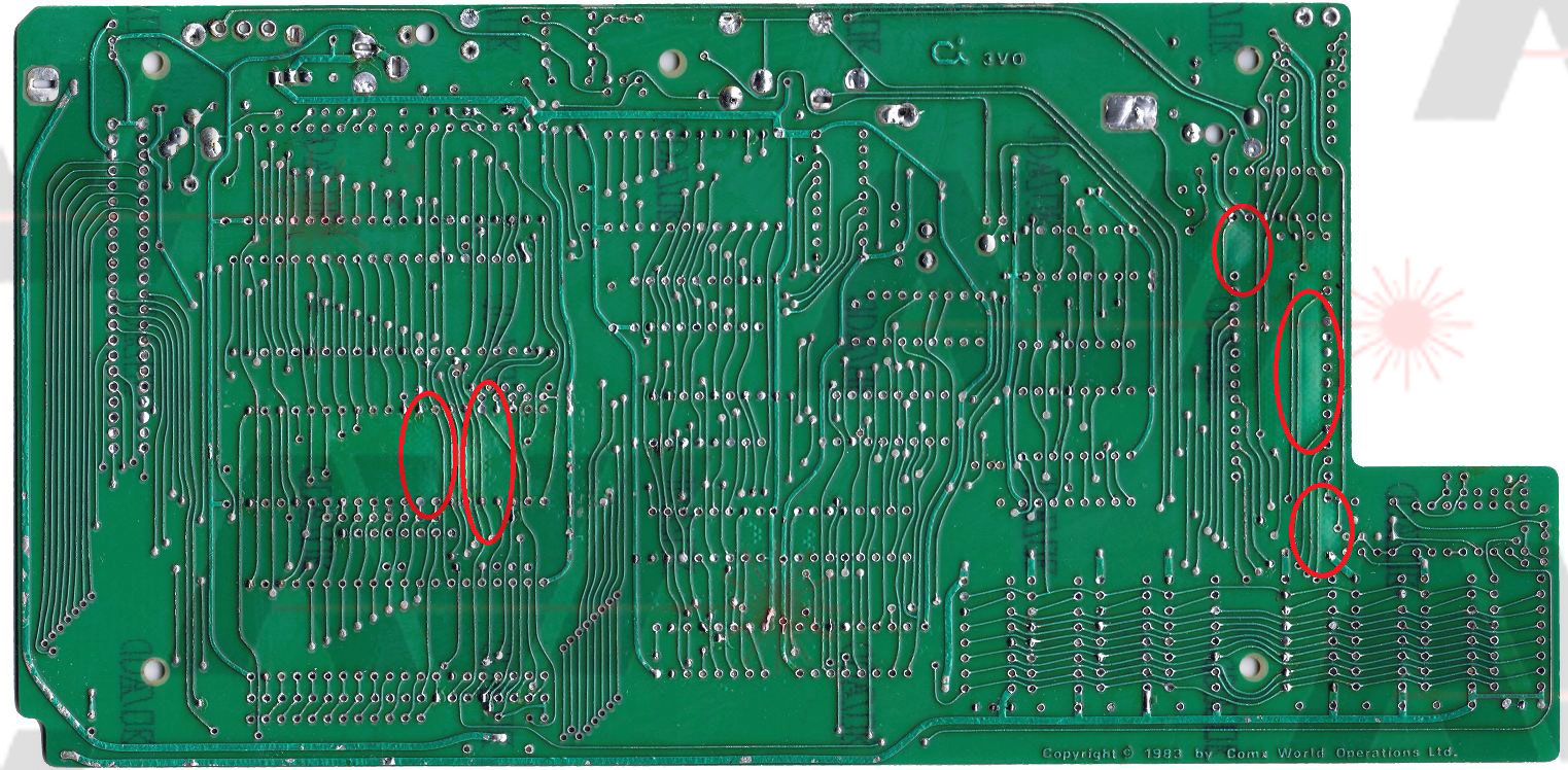
I updated the Super Board schematic with my notes from this version. At this point, I decided to start designing the next Super Board PCB.
SUPER BOARD (Rev2)
Second week of Nov
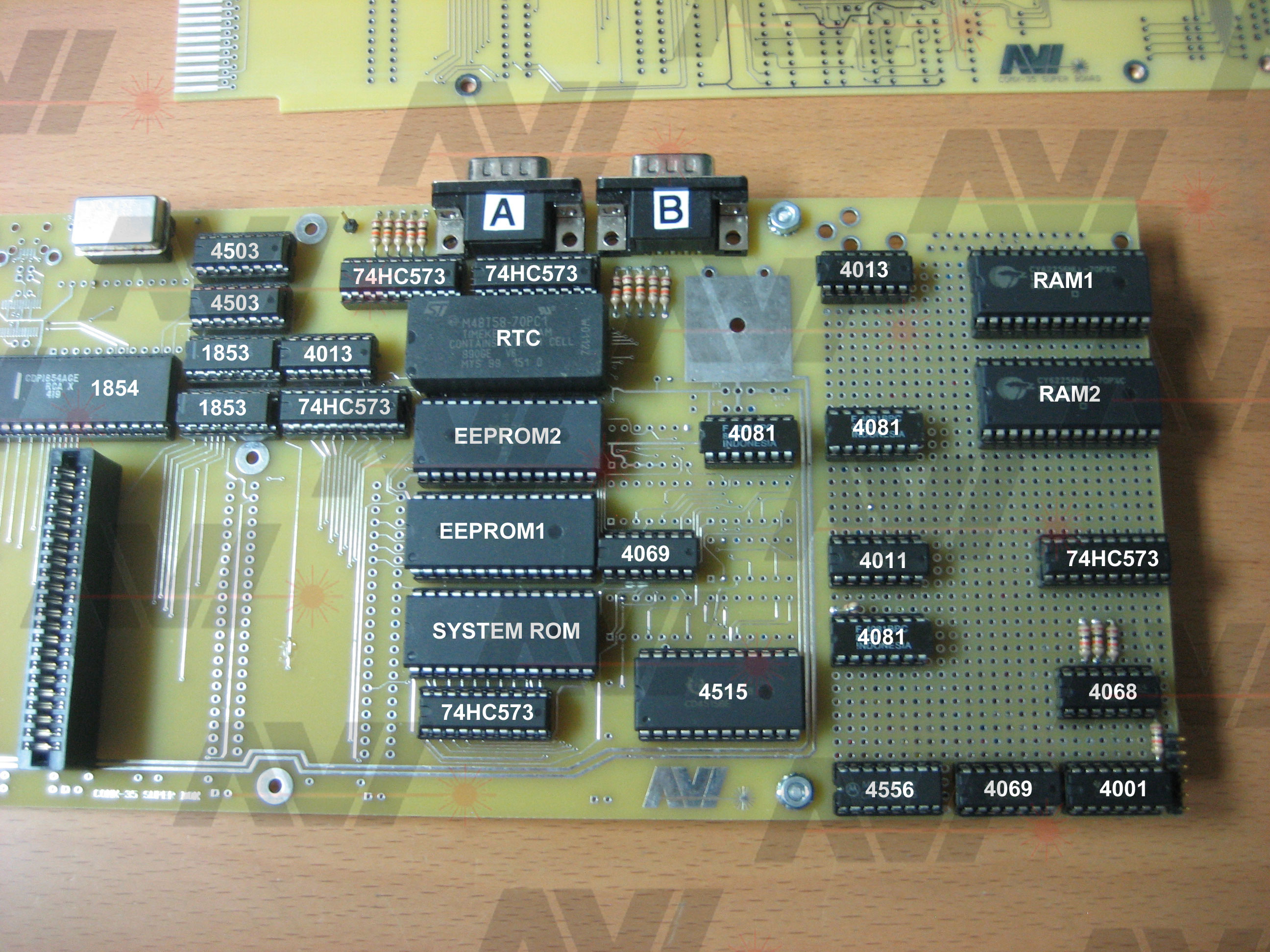
Using the newly drawn schematic as a guide, I made a first attempt at a new PCB layout:
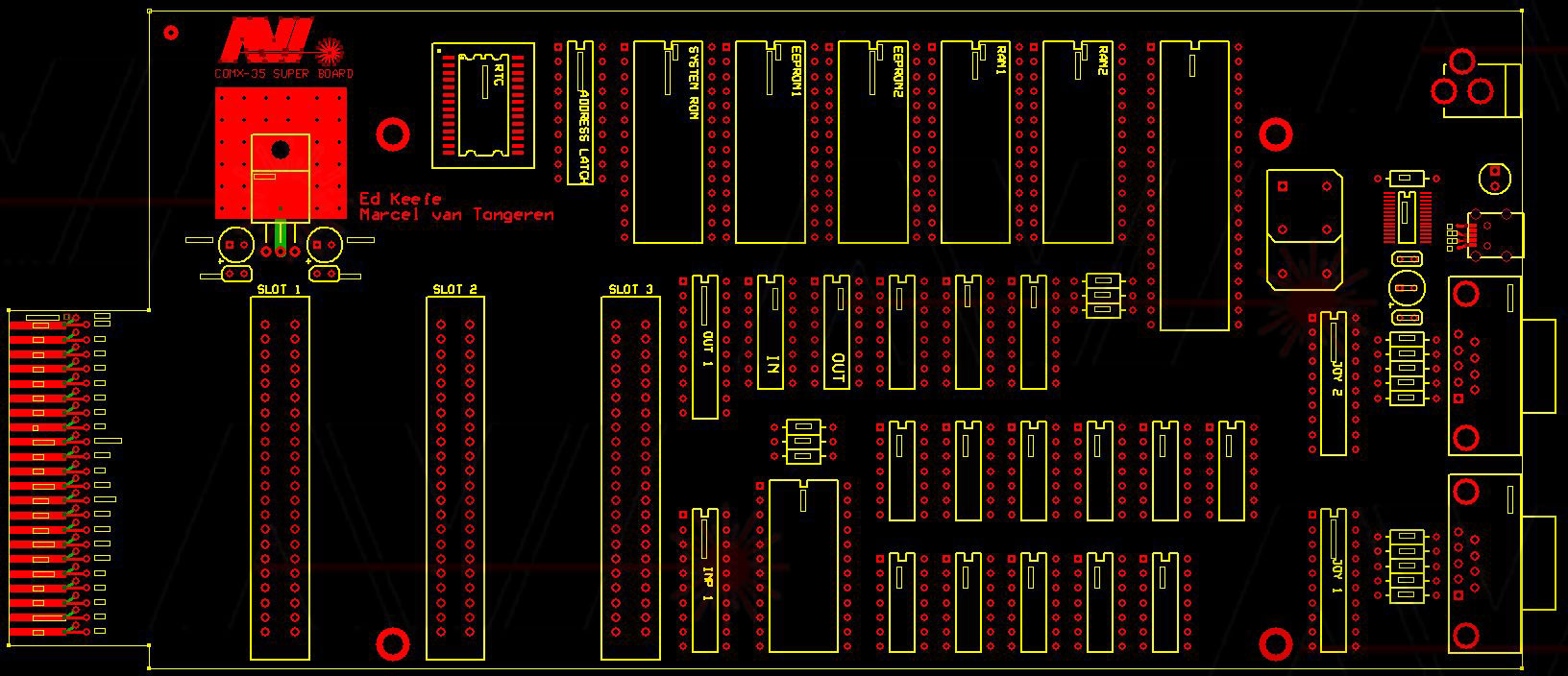
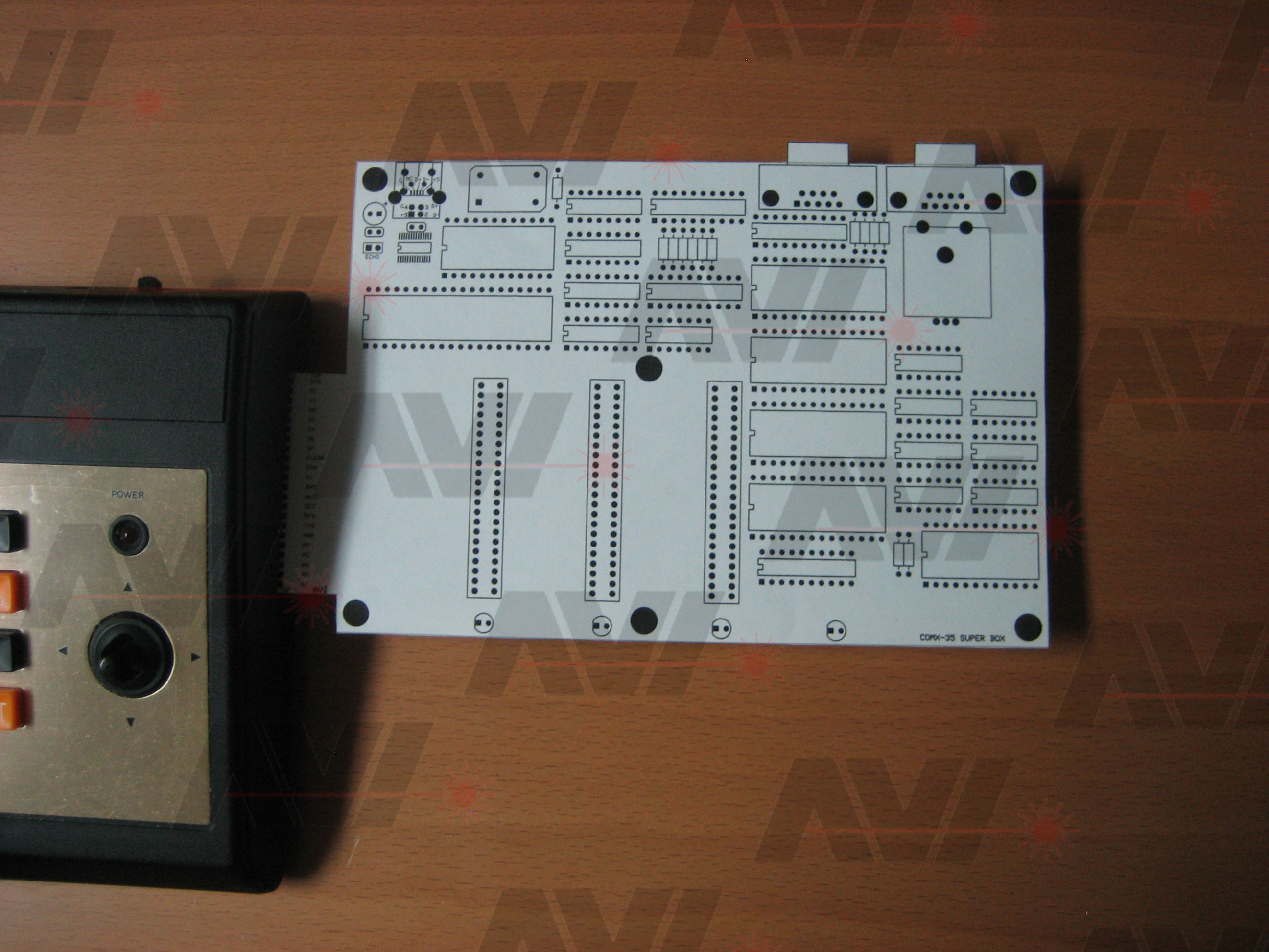
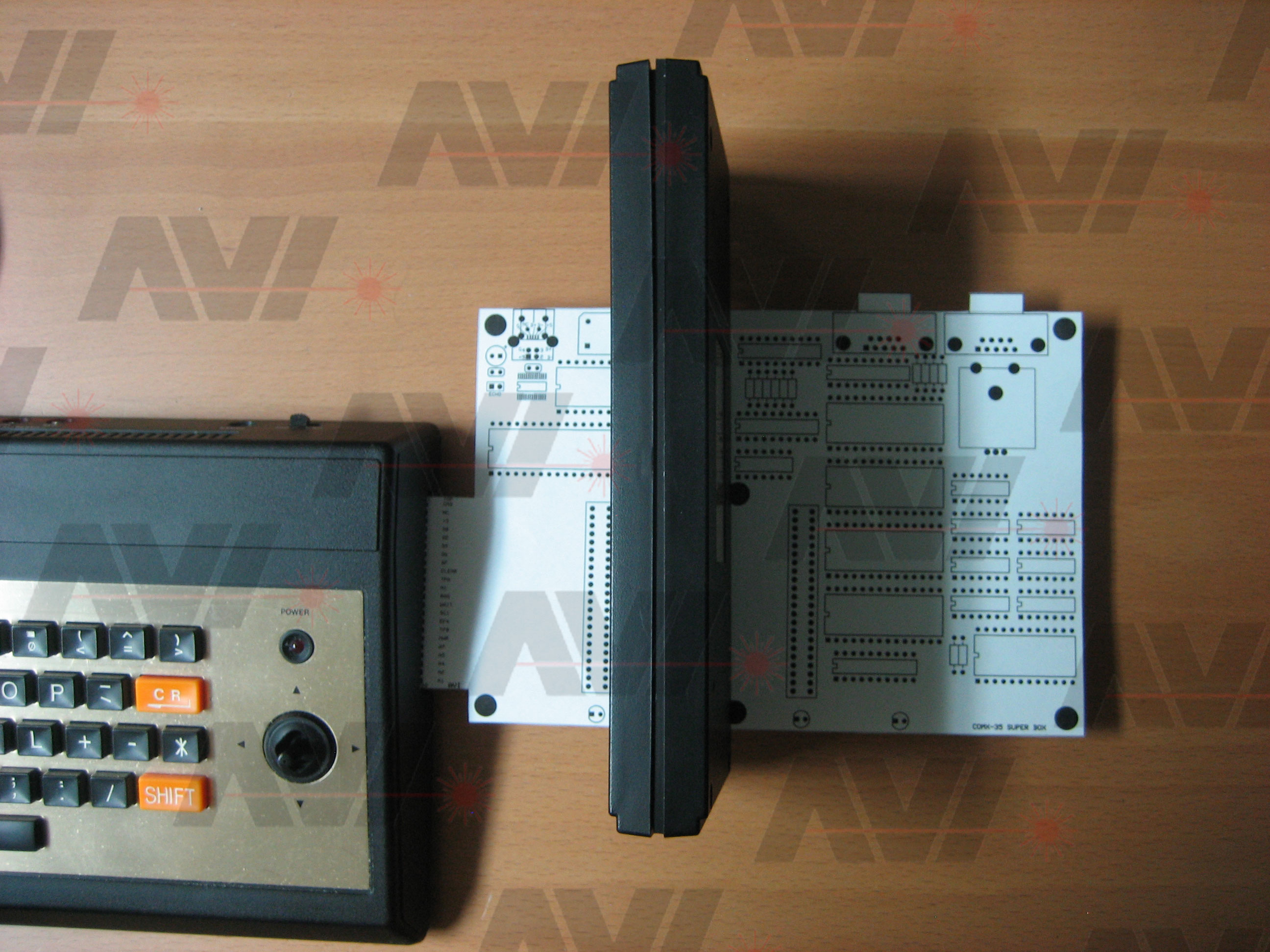
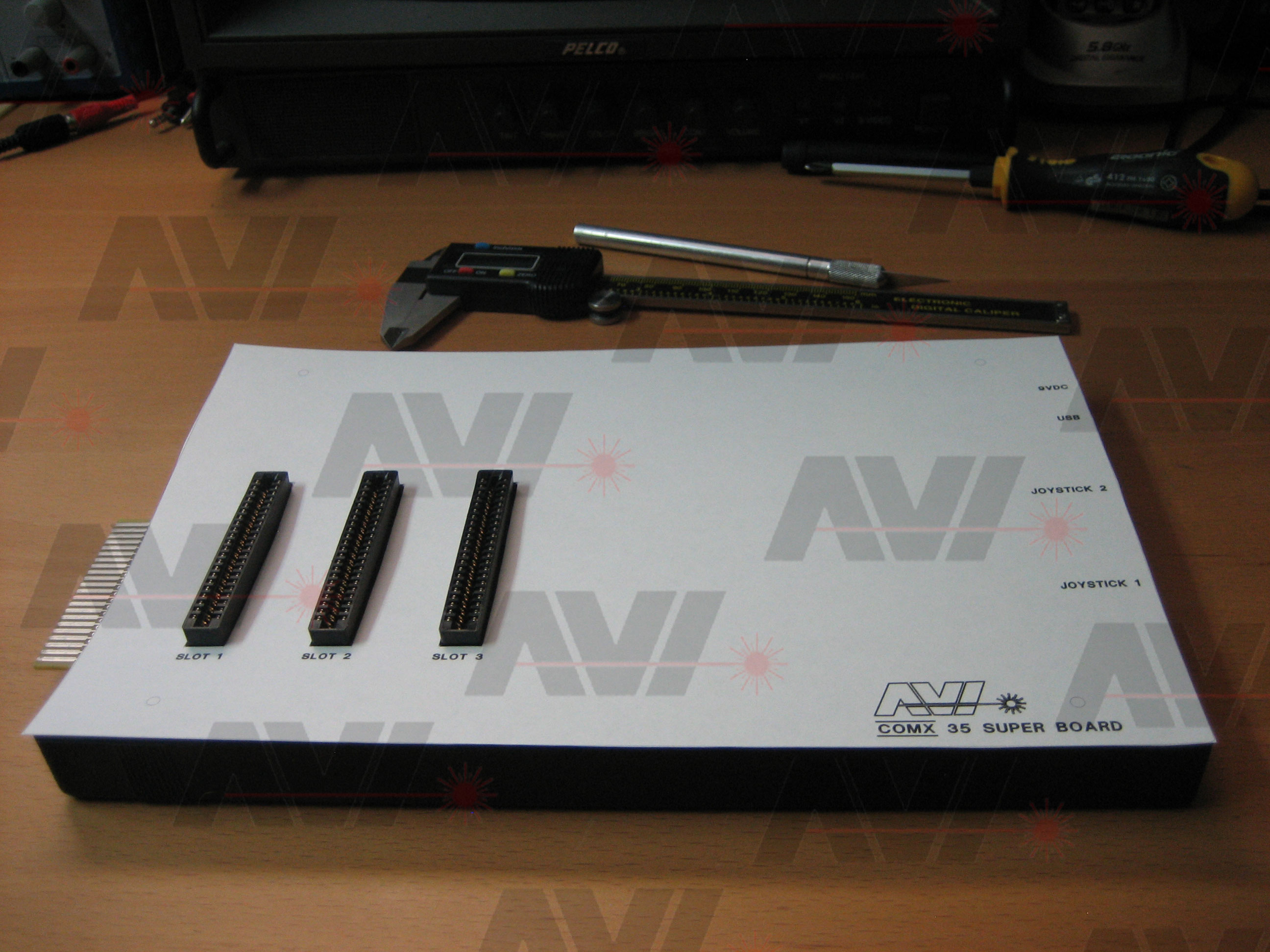
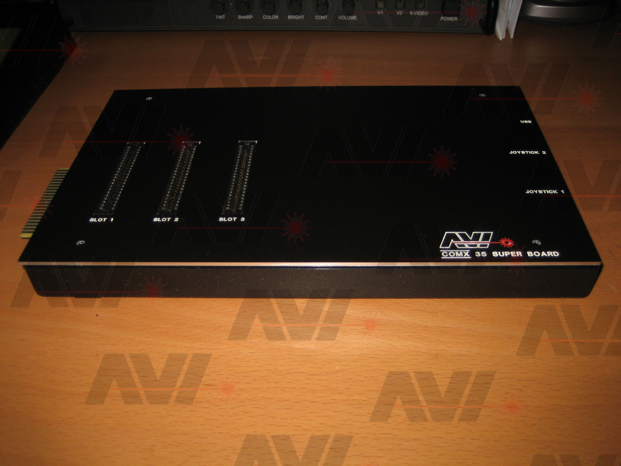
Based on the size of this layout, I designed the Super Board PCB to line up with the mounts in a stock plastic box available from Hammond manufacturing. I moved a few things around before ordering but it is pretty much the same. Here is the new PCB:
Bare:
Built (mostly):
I installed the board into the COMX and powered up. It worked! Well, everything except the USB section. The PC did not see the board when I connected the USB cable.
I found a couple mistakes on the PCB. I forgot to connect pin 19 of the USB FT232RL chip to the 1802 /CLEAR line. This caused the chip to not startup correctly. After fixing this the PC enumerated the board correctly. I could see PC data reaching the UART, but the loop back test was failing. I checked the circuit around the UART and found that pin 39 of the UART (/CTS) should have been connected to ground but was open. I repaired that and loop back now worked.
I went through the rest of the sections and everything worked.
I tried accessing different expansion boards in the Super Board slots. Slot 1 worked fine, but slots 2 and 3 didn't seem to work. I had the DS lines for slots 2 and 3 reversed.
At this point the Super Board just needed complete firmware.
FIRMWARE
As mentioned before the firmware has gone thru multiple changes, when writing this I worked on it for about 13 months and released 135 test versions to Ed. Ed's testing has been vital for me both when I didn't have any HW but also after I received the Super Board. Ed continues to support me with testing.
Now we actually have a semi-automated test suite which to some extent safeguards the quality of the existing code when I do make changes.
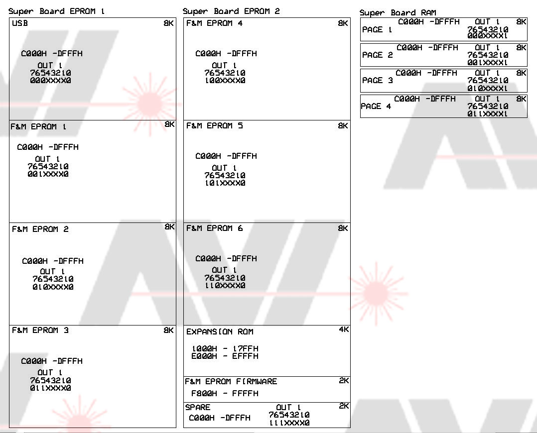
I don't want to bore everyone with all the changes and bug finding I have done, but would like to summarize the general structure of the Super Board. Before I start it is important to understand the COMX memory map and how the Super Board changes it:
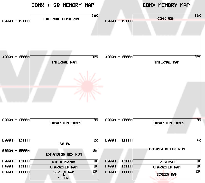
EXTERNAL COMX ROM
The internal COMX ROM is replaced with the new external COMX ROM. The changes in this ROM are limited, mainly jumping out of the ROM to Super Board firmware to start different routines to handle boot up improvements as well as USB, DOS and CARD command handling and the earlier mentioned bug fixes.
Also this ROM includes part of the 'old' expansion box ROM. The original expansion box copied address E000h-E7FFh to 1000h replacing part of the COMX ROM. This was also mainly done for 'CARD' command handling. This same ROM my brother and I already changed to allow jumps to the F&M Screen editor.
All this is in the external COMX ROM inside the Super Board. Leaving memory E000h-E7FFh available for Super Board firmware.
INTERNAL COMX RAM
The internal RAM is not changed, however the firmware does use some RAM. I have tried to limit this as much as possible to avoid issues with existing firmware or other expansion cards.
The following addresses are used:
- 42A0h: Used by COMX BASIC for start address of latest used command. firmware uses this in certain cases to detect what type of command is being used. For example to differentiate between PRINT USB Q and A=USB Q.
- 42A1h: Used during command handling to 'save' R8.1.
- 42A3h-42A6h: Subroutine call to the requested USB or DOS command. The same locations are also used by COMX BASIC for some command handling subroutine calls
- 43F7h: Used by the F&M Screen Editor
- 43F8h: Used by the F&M Screen Editor, 0 screen editor, 1 line editor
- BE80h-BEFFh: DOS buffer but also used by USB commands for the USB PC <-> COMX buffer. Also used by some USB commands (WORM, TENNIS, HIT, SPACE, MON, DMON) for storing temporary data.
- BF42h: Current OUT 1 value (selected slot/bank)
- BFFDh: Printer slot if connected
- BFFEh: OUT 1 value (selected bank/slot) at USB/DOS command entry
SUPER BOARD firmware
The Super Board firmware is spread over different locations:
E000h-E7FFh and F800h-FFFFh which are always available (no slot or bank switching needed).
C000h-DFFFh which is switched between slot 1 to 4 (When slot 4 is selected, between bank 0 to 7).
USB Command entry starts at F800h.
F800h-FFFFh as well as E000h-E7FFh areas are mainly used for:
- - The slot and bank switching routines
- - Boot-up routines
- - Extended interrupt for clock and JOYLOAD handling
- - Simple hexadecimal to decimal converter
- - Extended screen editor features (CNTL-R, X, V)
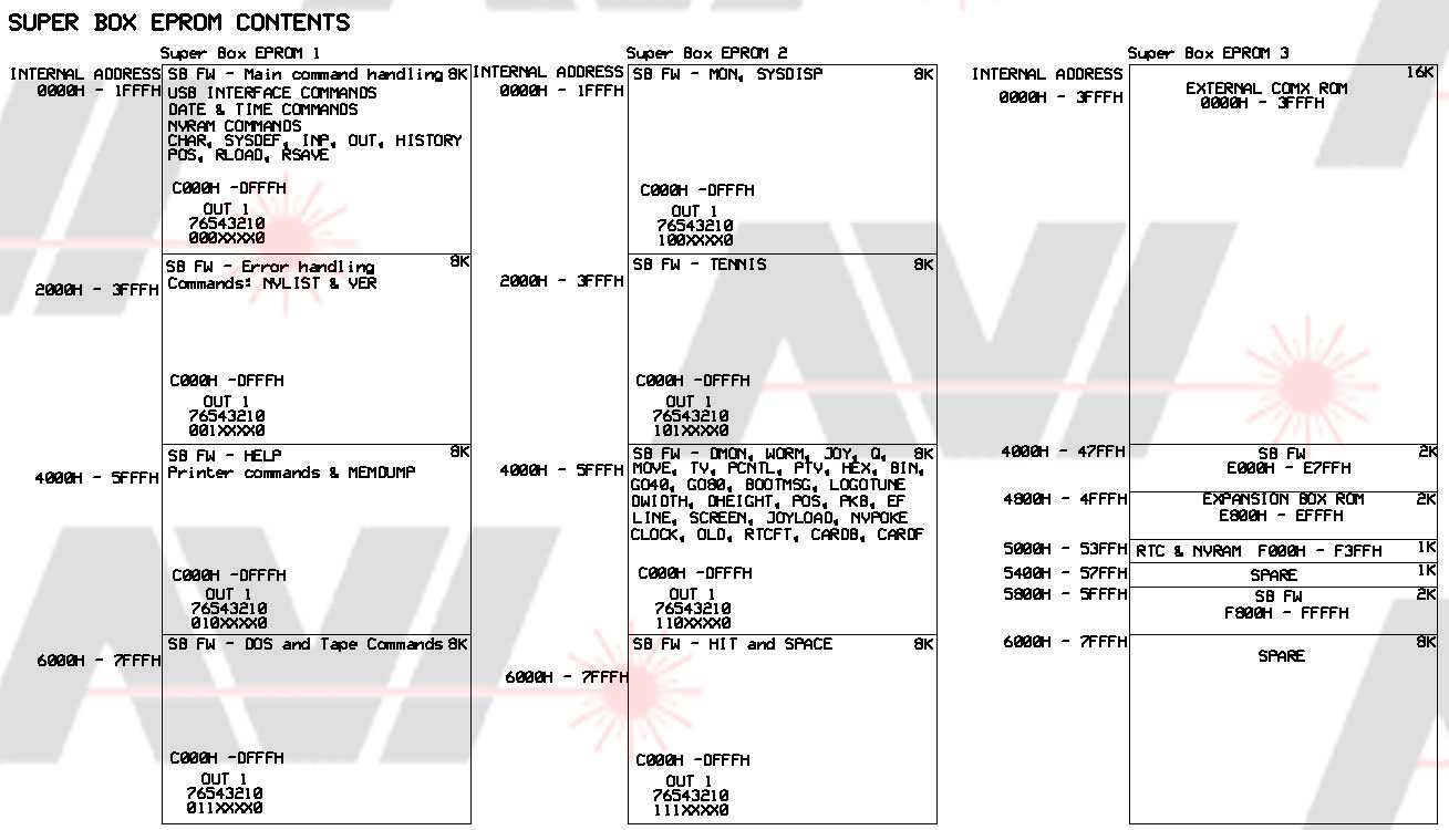
Super Board slot 4 is broken up into eight 8KB ROM banks and eight 8KB RAM banks. All of the banks are in the C000h-DFFFh range and selected individually.
ROM bank utilization:
- Bank 0. Main command handling.
- USB Interface commands
- DATE and TIME commands
- NVRAM commands
- Including these commands:
- CHAR
- SYSDEF
- INP
- OUT
- HISTORY
- POS
- RLOAD
- RSAVE
- Bank 1. Error handling and all error code text.
- NVLIST
- VER
- Bank 2. HELP command and all HELP text
- Printer commands
- Including:
- MEMDUMP command
- Bank 3. DOS and TAPE commands
- Bank 4. F&M Monitor (MON) and SYSDISP
- Bank 5. Tennismania (TENNIS)
- Bank 6. F&M Disk Monitor (DMON) and Eat a worm (WORM)
- Including these commands:
- JOY
- Q
- MOVE
- TV
- PCNTL
- PTV
- HEX
- BIN
- GO40
- GO80
- BOOTMSG
- LOGOTUNE
- DWIDTH
- DHEIGHT
- POS
- PKB
- EF
- LINE
- SCREEN
- JOYLOAD
- NVPOKE
- CLOCK
- OLD
- RTCFT
- CARD B
- CARD F
- Bank 7. Hit and Run (HIT) and Space Invaders (SPACE)
RAM banks 8 to 12 are never used by the USB firmware. Bank 13 and 14 are used by DOS DISKCOPY and FILECOPY and any data stored in them will be overwritten when those commands are executed.
RAM bank 15 is used for RAM swap area mainly for DOS commands, data storage for DMON, MON and TENNIS and CNTRL X, V and R buffers.
NVRAM
NVRAM is divided like this:
F000 Fxxx: User area.
This area can be used by any user or user program. No defined format is available so any address location can be filled as desired. USB NVPOKE can be used to store data and COMX BASIC PEEK can be used to retrieve data. Fxxx is defined via USB NVSTART.
Fxxx F3E7: software area.
This area can be used by any software. The area is formatted so every software program can find stored data back. USB NVPUT, NVGET, NVIGET, NVSGET, NVCLR and NVDEL can be used to store, retrieve or manipulate data to/from this area.
F3E8 F3F7: System area.
Reserved for use by the Super Board firmware. Maybe link to a document with the explanation of all system locations?
F3F8 F3FF: Reserved for the RTC.
Last week of Nov
While waiting for new firmware to test, I started thinking about how to case the Super Board. The Hammond box I selected is really too tall, but it was the only one that fit length and width. While I had the Super Board mounted to the bottom half of the case, I noticed that other than the slot connectors everything else was below the top edge of the case bottom.
I dragged a ruler across the Hammond case just to be sure. I thought maybe I could just add a flat cover as the top of the case. Something like this:
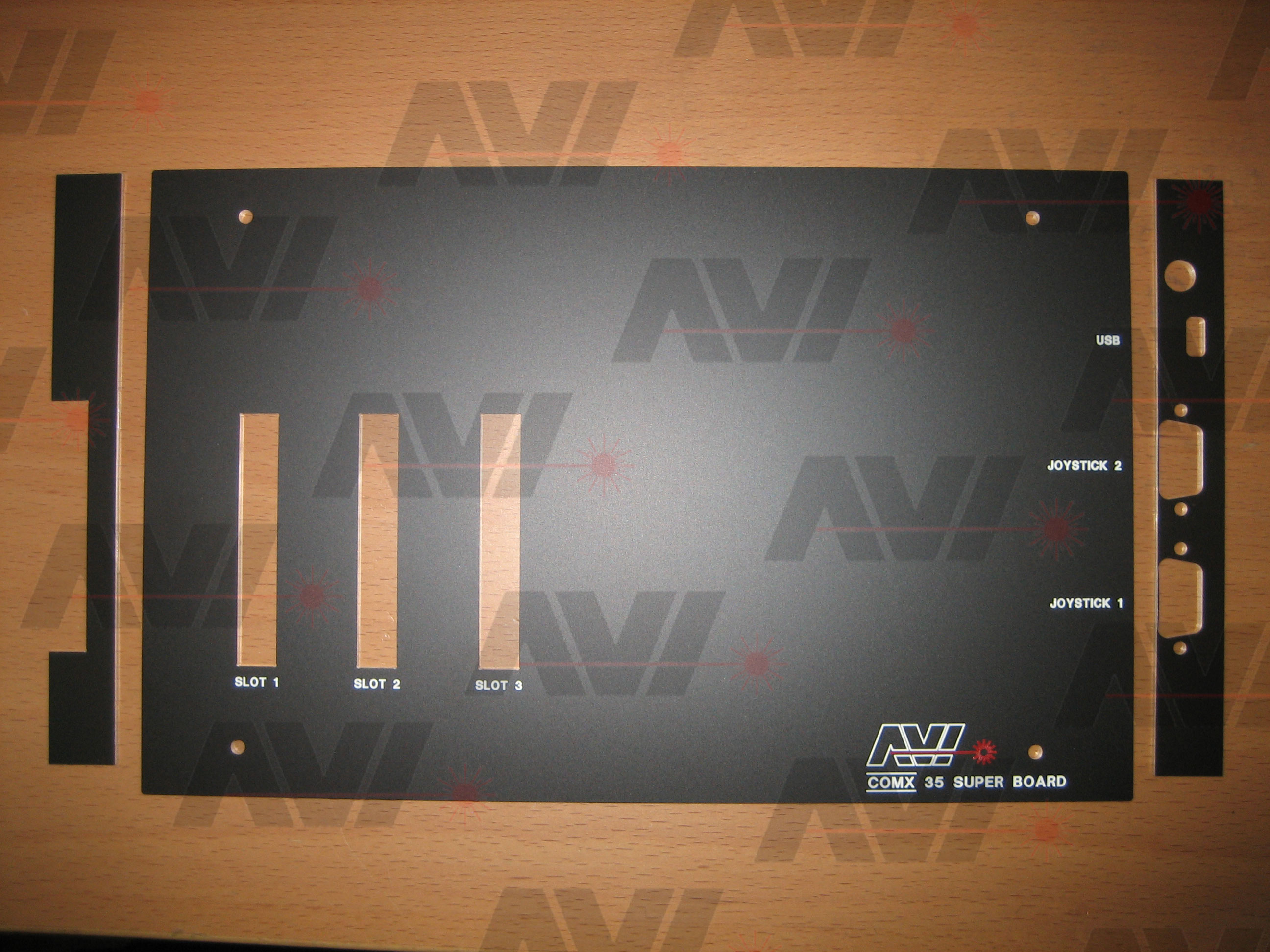
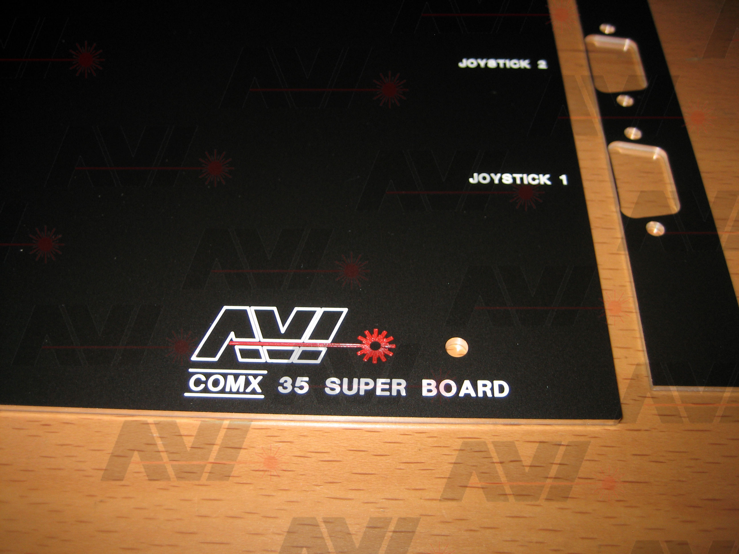
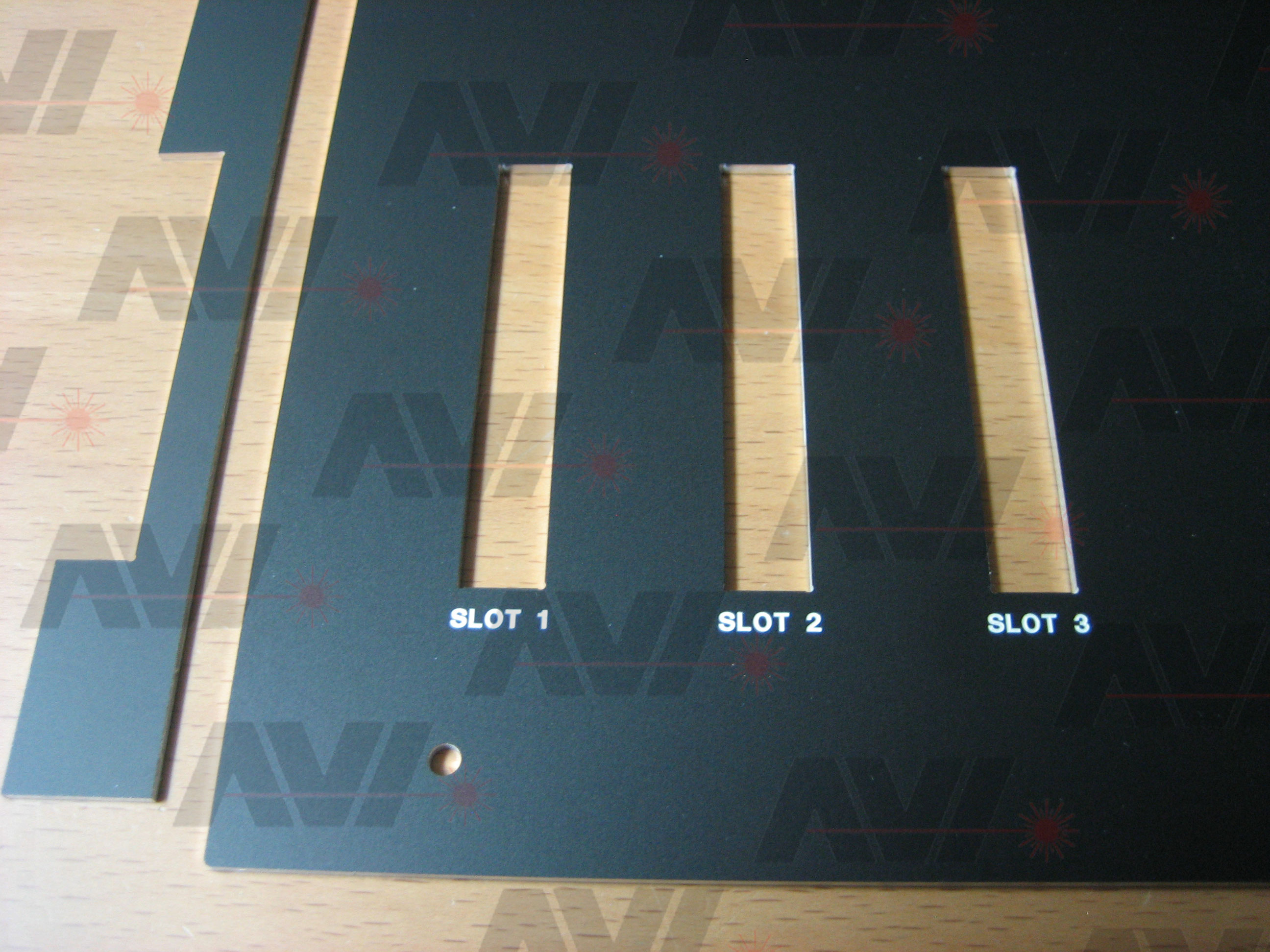
With this in mind I drew up a top panel in Adobe Illustrator. I printed it and cut it out. Here is what I came up with:
I further refined the design:
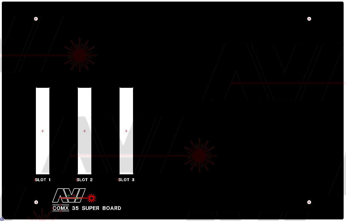
I added some more text:
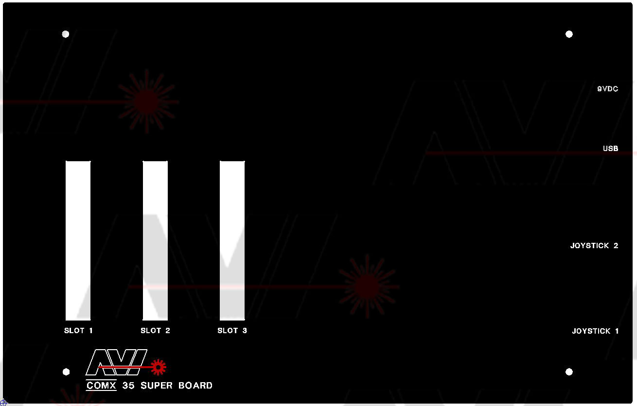
I adjusted a few things and made a measured drawing of the panel. I then drew up a couple of end caps.
First week of Dec
I used the software provided by Front Panel Express (http://www.frontpanelexpress.com) to draw up the three panels. I placed an order and a bit later received these:
Middle of Jan 2013
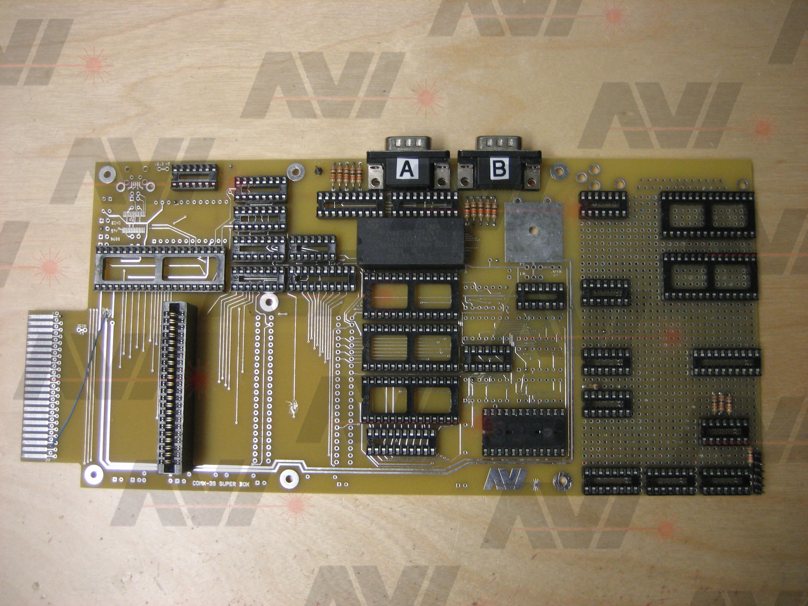
With the panels in hand, I built a second Super Board and sent it to Marcel.
Late Apr
Some time after shipping it, I realized I had not tested the tape read and write functions of the basic COMX-35. Using USB from my PC, I loaded a small program into the COMX and saved it to a small mp3 voice recorder I have. I checked that the track recorded, it sounded fine.
I swapped the audio cable, issued the load command and pressed play. I waited, watching the timer on my voice recorder, until the file finished loading but the COMX never indicated that the file was loaded. I cycled power and tried again. Same thing. I did a list command nothing was loaded.
I removed the Super Board and tried one more time. The file loaded fine.
On the COMX, EF4 is used as the tape input. On the Super Board EF4 is used to monitor the UARTs "Data Available" (/DA) and "Transmit Holding Register Empty" (/THRE) lines. I have a special circuit in place so the single EF line can serve double duty.
I cut the EF4 line on the Super Board and reinstalled it in the COMX. I loaded the tape without error.
It turns out I had overlooked the EF4 line when I designed the tri-state control section. EF4 should only be active when the Super Board is selected. If any other slot is selected, EF4 should be made available to the board installed in that slot. While the Super Board is selected, the tape input is not usable.
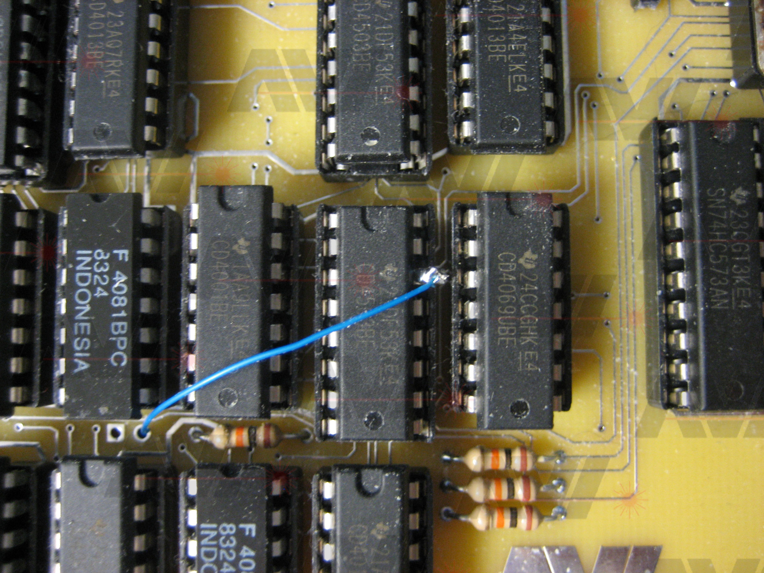
All three of the wires in the first picture below are for fixing EF4 problems. The horizontal wire is the tape fix. The other two are for a problem with COMX floppy cards. You can read about that here:
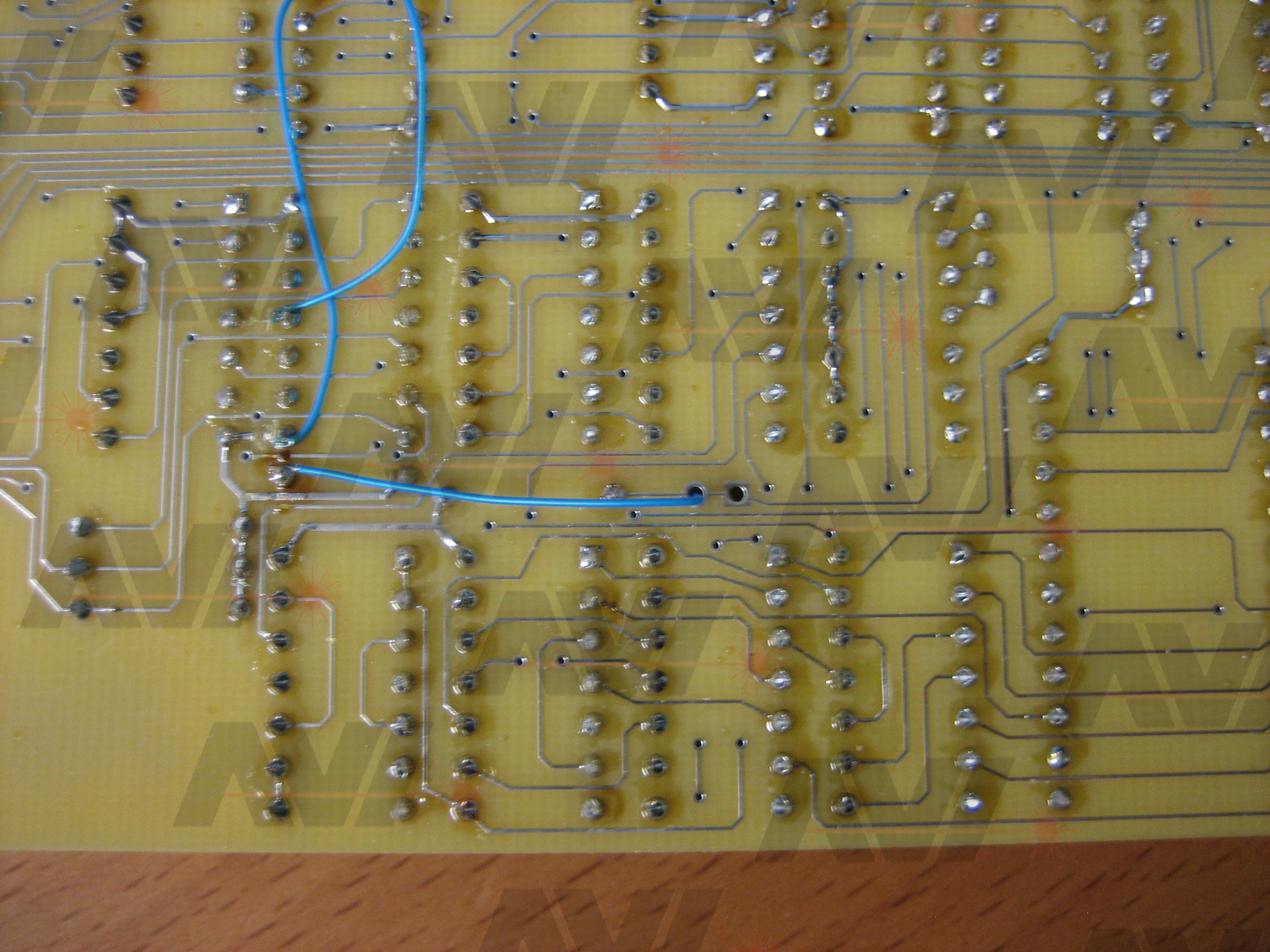
I sent instructions to Marcel on how to do the repair. He made the fix and now his board is also working.
With this last error corrected, I believe that the Super Board is complete.
SUMMARY
I once again updated the Super Board schematic from my notes.
Marcel continues to write firmware and I continue to test his code. Just when we think we are done, we think of something new to add.
If you would like to discuss any of the projects on this site, or the COMX-35 itself, we have created a Yahoo Group just for that. Please feel free to visit the COMX35 Yahoo Group page located here:
http://tech.groups.yahoo.com/group/COMX35/Thank you for reading this. I hope you found it interesting.
ED & Marcel
DOWNLOADS
Here are some documents for further reading:
Superboard Manual Memory Details RAM & NVRAM Header Format Error MessagesAs development continues, these documents will change.