AVI COMX-35
EXISTING TECHNICAL INFORMATION
I asked my friend in Sweden (Marcel) if he had any information I was unlikely to find on the Internet. He said that two different schematics existed for the COMX-35.
He sent me a two page schematic which is a larger version of the one in the "COMX Technical Manual" (http://www.comxclub.hobby-site.com/COMX35TechnicalManual.pdf) which was unreadable. This larger version was not much better. Pin numbers are almost impossible to read.
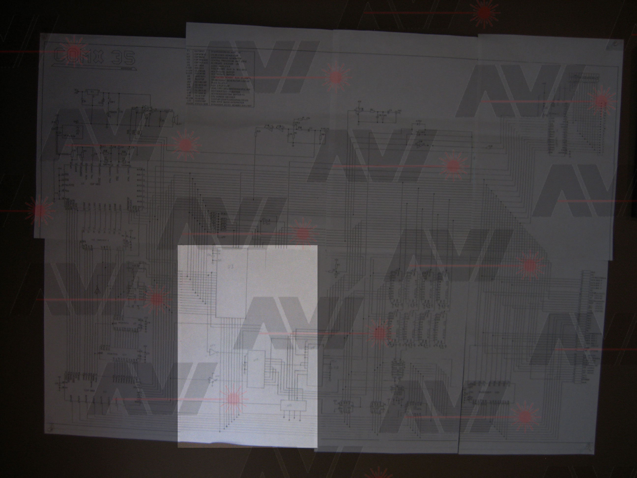
Luckily, or so I thought, Marcel also sent me a set of seven pages that formed a very large version of the schematic. The biggest problem with this version was that it was seven of eight pages. Marcel explained to me that he and his brother (http://www.emma02.hobby-site.com/comx_fandm.htm) made extensive use of that particular page and over time somehow lost it.
The missing page would have contained the processor, timing, address decoding and interrupt handler. The schematic is in a 4 sheet x 2 sheet form. The missing page was the second from the left on the bottom row.
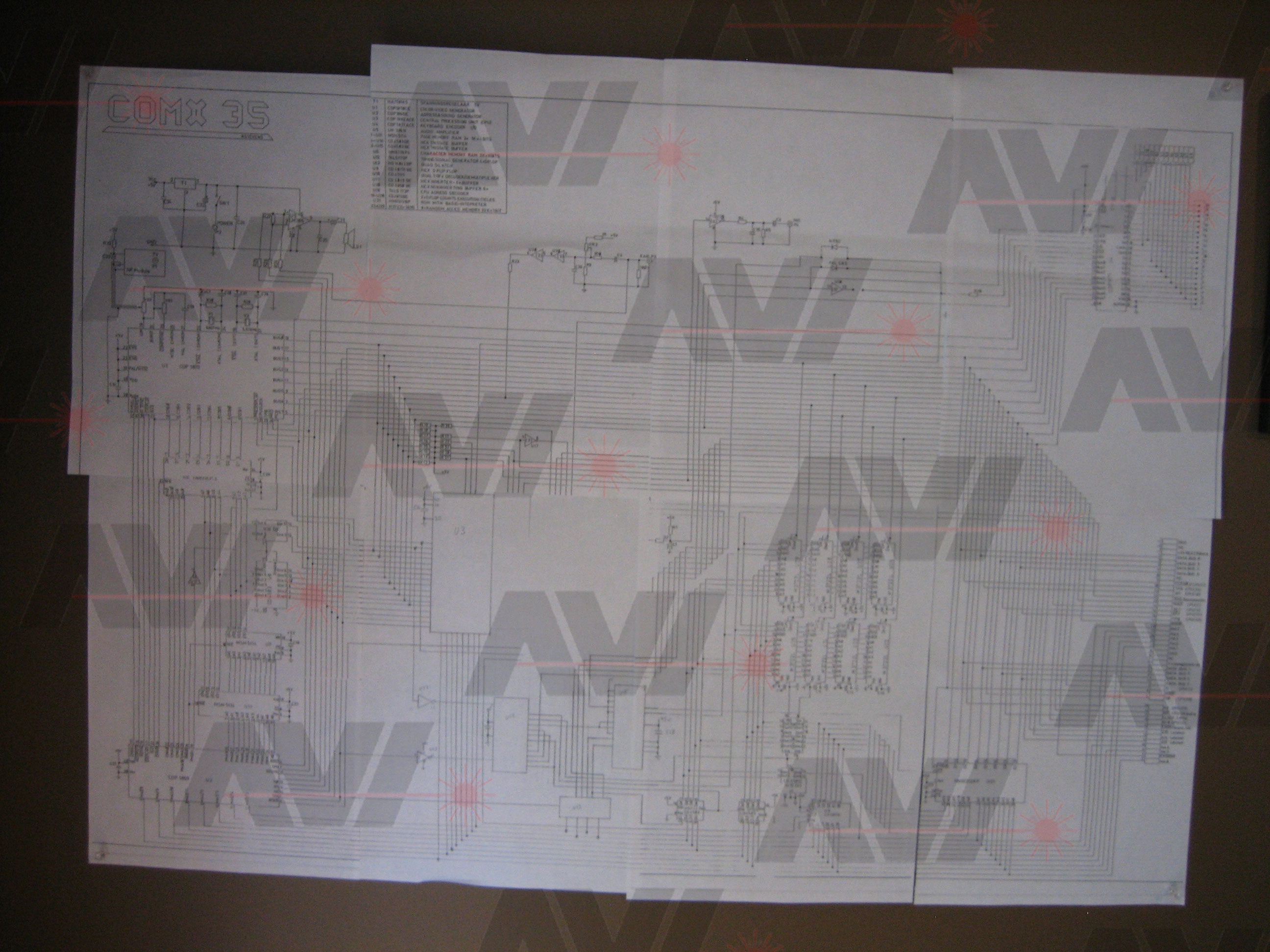
I was so thankful Marcel made this available to me that I committed to drawing the missing page. I began to do just that. I printed out the pages and used Photoshop to make them line up as good as I could. I then added a blank page and began using the two page schematic to fill in the missing information.
It became apparent that they were not the same schematic and there were some errors on the 7 page version.
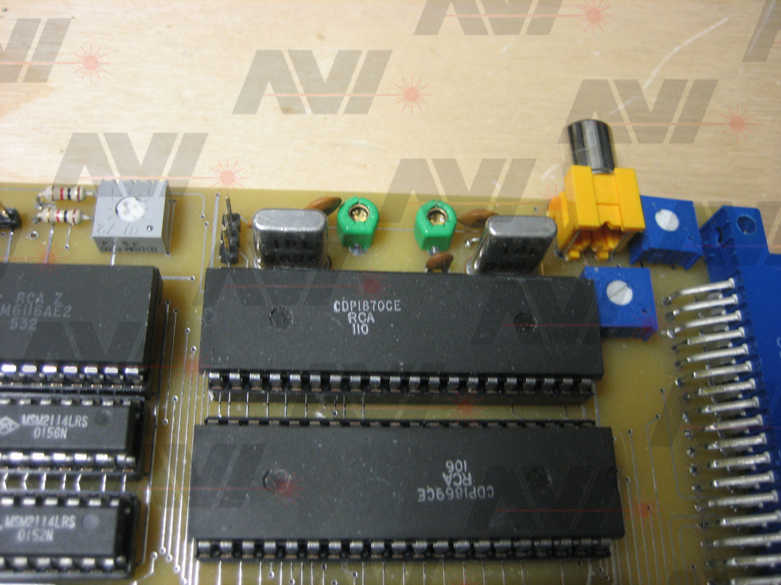
Here is an example of what I am talking about. The 8-page schematic was not trustworthy. There are many places where the pin-outs of chips are not correct. I don't mean off by one pin or some sort of transposition error, I mean it looks like it was done on purpose to confuse potential competitors. For example, the pin-out of the ROM is wrong. Here is a picture of what the large schematic shows:
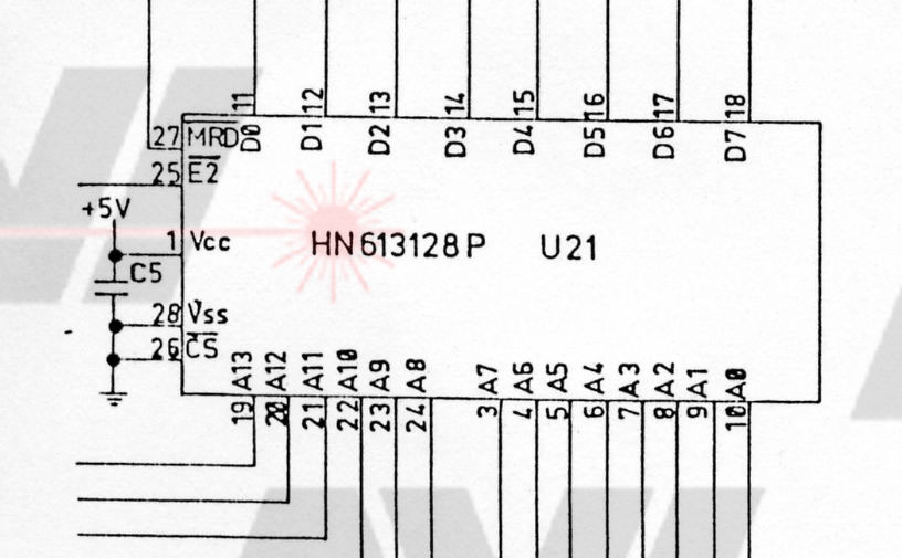
and here is the pin-out from the datasheet for the ROM:
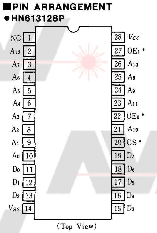
Based on this error and numerous others, I decided to redraw the entire COMX-35 schematic myself.
NEW SCHEMATIC
I had purchased a used COMX on eBay that would power up but had no function. I removed the PCB from the bottom of the case and removed the top, keyboard portion by de-soldering the 20 wire cable.
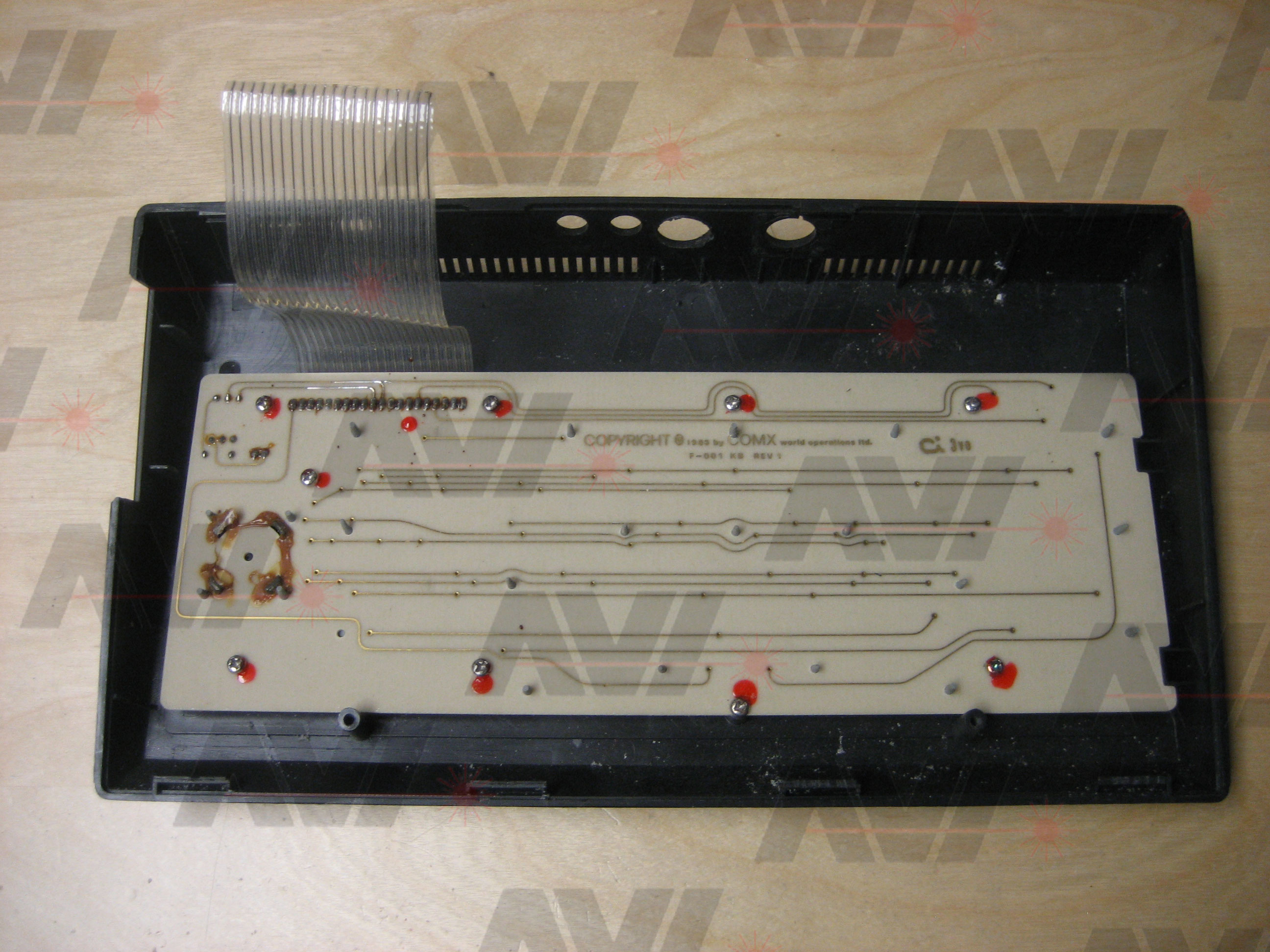
I was left with just the main PCB.
I used this board to verify the ROM pin-out described above, by "beeping" it out with an ohm meter (used as a continuity tester). The COMX-35 board matched the datasheet for the ROM. The little 2 page schematic for the COMX seems to be correct but it is very hard to make out the pin numbers.
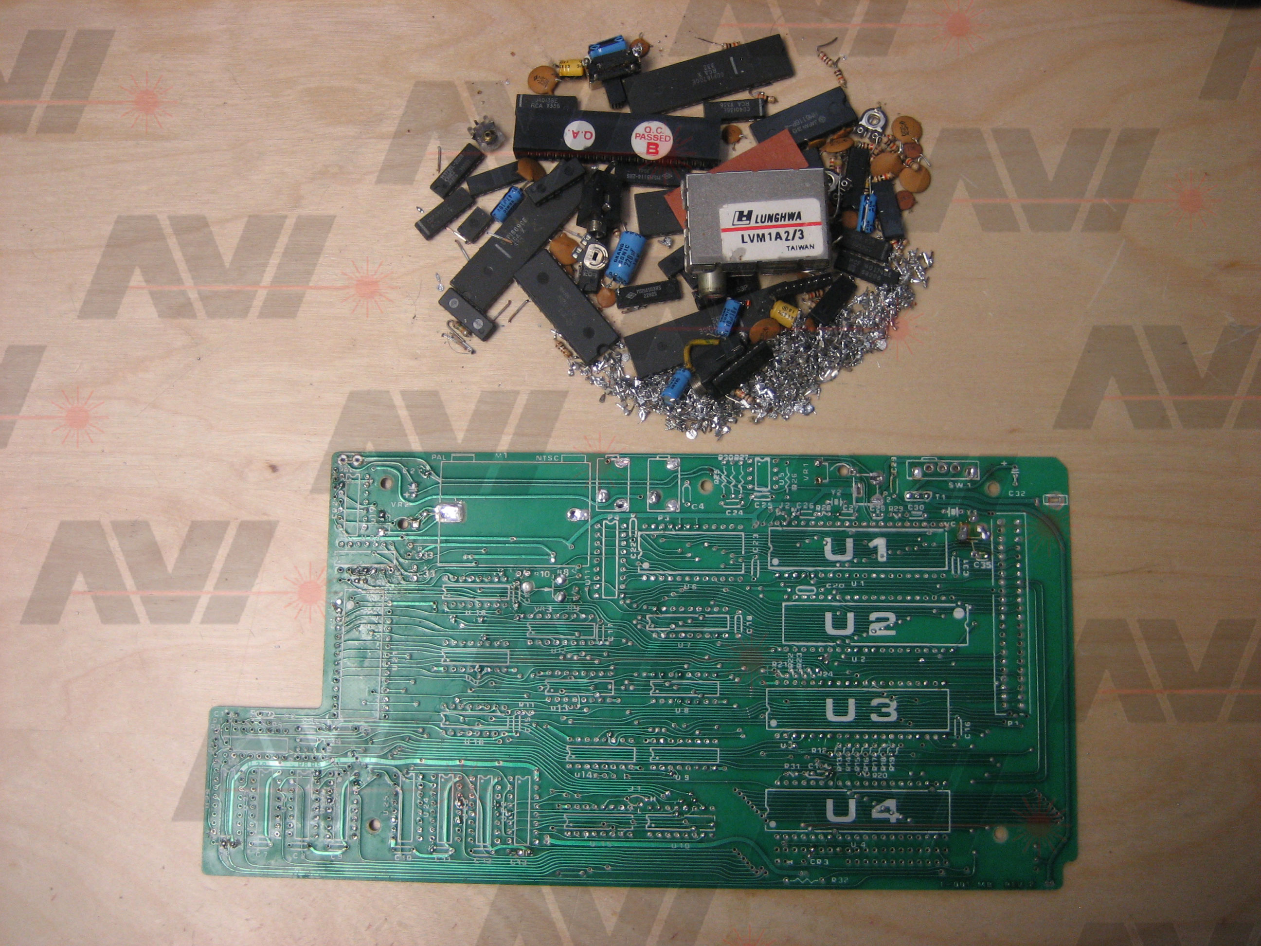
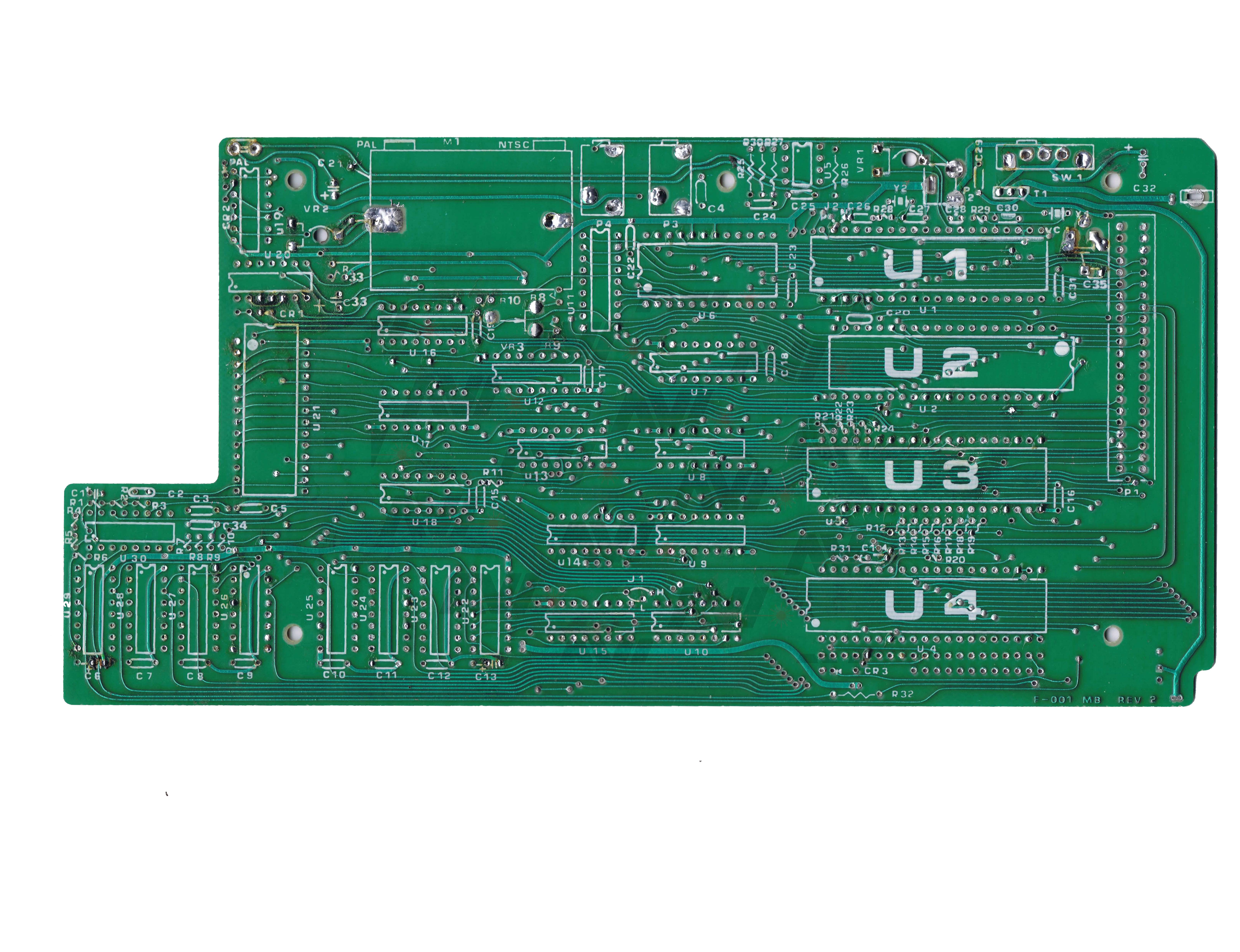
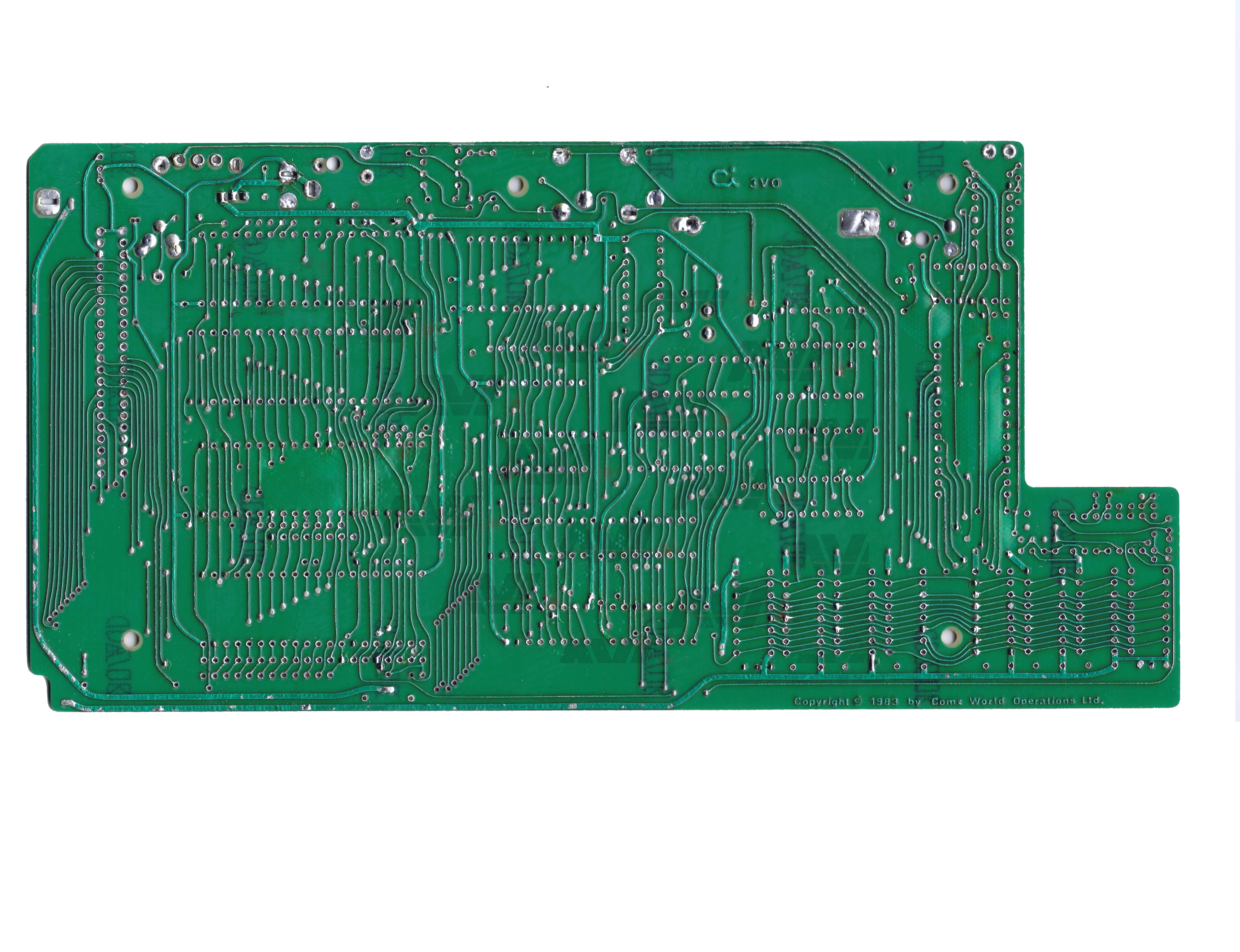
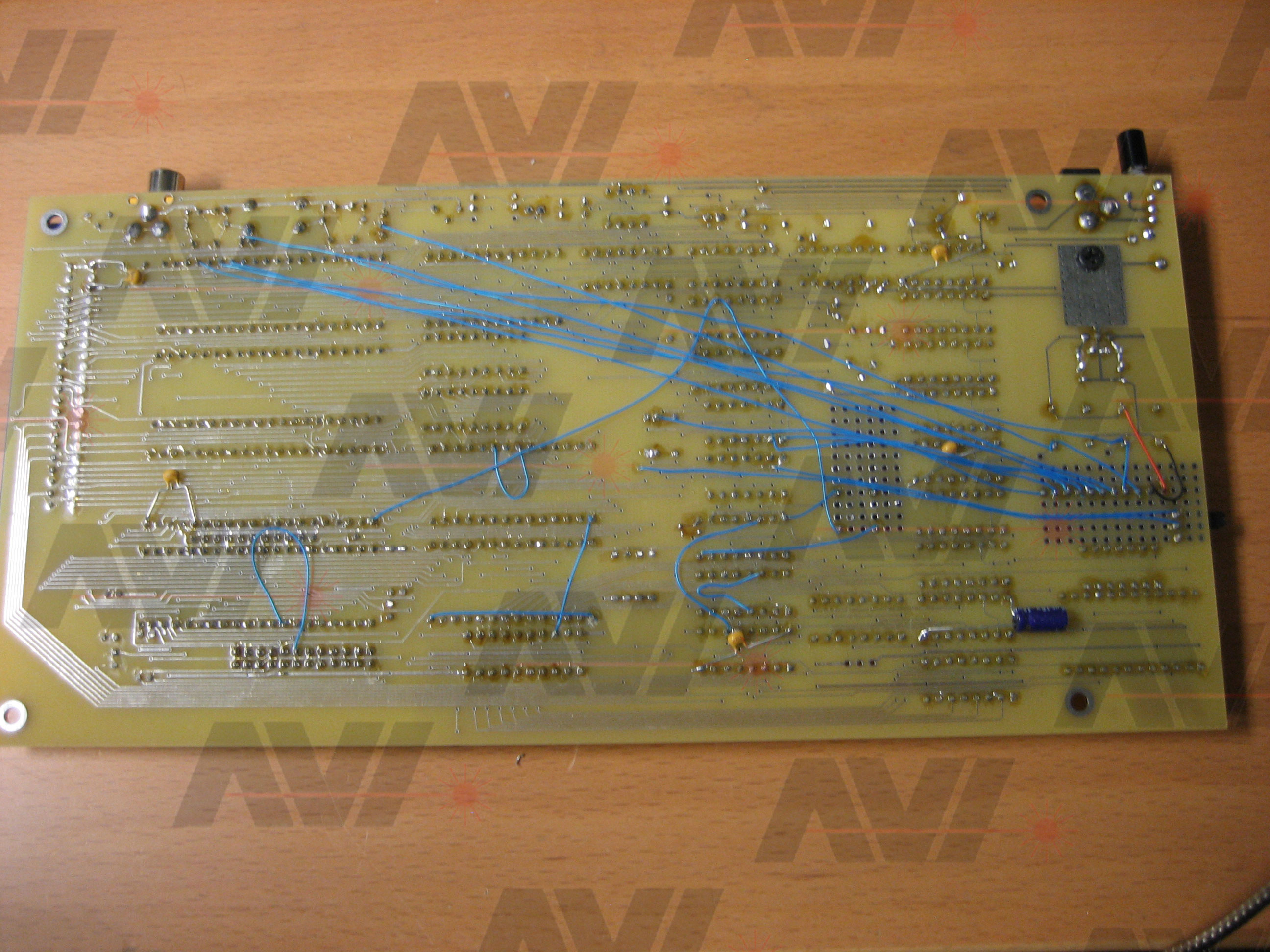
To have better luck tracing out the COMX-35, I removed all the components and was left with a bare board.
Here is what I call the COMX-35 "kit":
I know this is sort of sacrilege, but I figure it is for the greater good. I would end up with a perfect schematic of the COMX-35.
A previous owner tried to repair the board and in the process de-laminated the board in a few places (The light green areas).
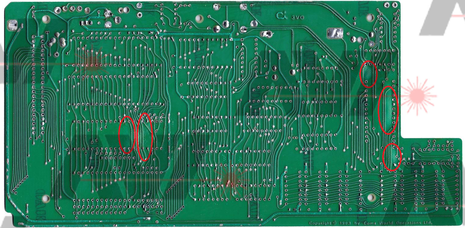
Since I wouldn't be trying to fix it, I chose to make a good set of scans of the PCB.
After a bit of work, I finished drawing up the board on a bunch of sheets of paper.
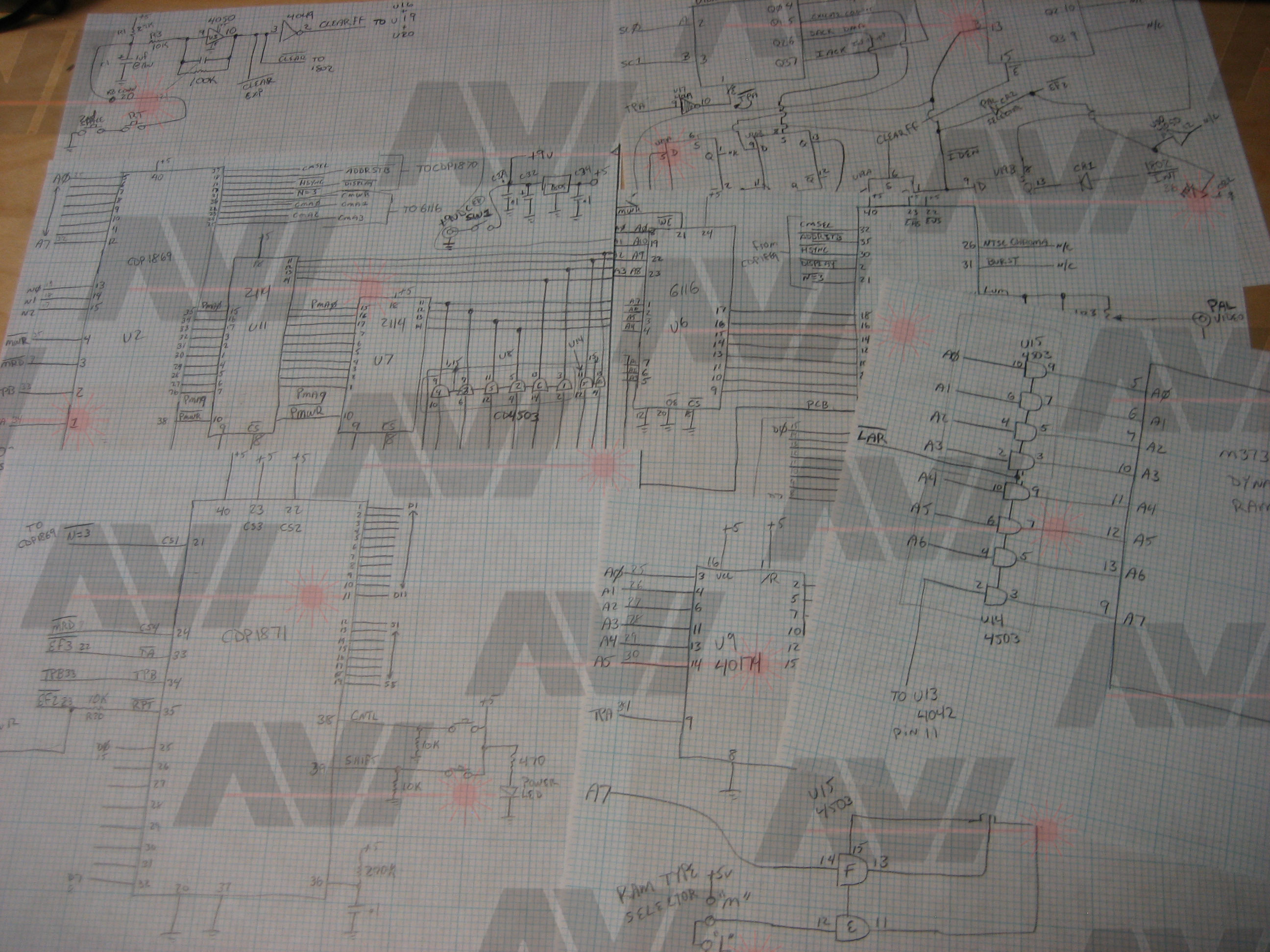
From these drawings I finished formally drawing up a schematic of the COMX-35.
Using this schematic as the reference, I "beeped" out the PCB, checking for omissions and mistakes. I found a few and updated the formal schematic as I went on. I was satisfied that I had a good schematic now.
I decided to build a COMX-35 from this schematic to verify I had it correct. There is no better way to prove a schematic is correct than to build it up.
AVI COMX-35
I decided to make a few changes and additions to my version of the COMX-35. Here is a list of them:
- Static RAM
- Alternative address decoder
- Real keyboard
- No modulator
- Video jack
- Volume control
- PAL / NTSC selector
RAM
The original COMX had 32K of Dynamic RAM using 8 OKI M3732 chips. These are still available on the surplus market, but it would be simpler to use one 32Kx8 Static RAM chip. I decided to add a 62256 RAM chip to the design.
My plan was to get the system working as I drew it in the COMX-35 schematic first, including the Dynamic RAM. Once I had it running I would start adding the components for the AVI version of it.
ADDRESS DECODER
After drawing up the COMX address decoder, I decided to add an address decoder of my own design. The COMX uses four chips to do the decoding, mine uses two.
What I didn't understand when I designed my decoder was that the /CAS and /RAS signals required by the Dynamic RAM were also generated by the COMX-35 address decoder. My circuit would work for the ROM and Static RAM but would not generate the proper refresh signal required by the DRAM. When I designed the PCB I left my decoder on the board to experiment with.
I made my final updates to the AVI COMX-35 schematic:
OTHER ADDITIONS
Adding a volume control was as easy as replacing a fixed resistor with a potentiometer. Same with the video jack, since I was leaving out the modulator I hooked the video to a yellow RCA connector instead.
I will talk about the keyboard a little further down on this page.
The PAL / NTSC selector was not drawn into the AVI COMX-35 schematic. I do have this working, but in a crude way. You can read about it later on this page. I designed the AVI COMX-35 to be in PAL mode. I am in the US but I wanted my COMX to match the dead one I had. I also have a PAL monitor so it is not really a problem.
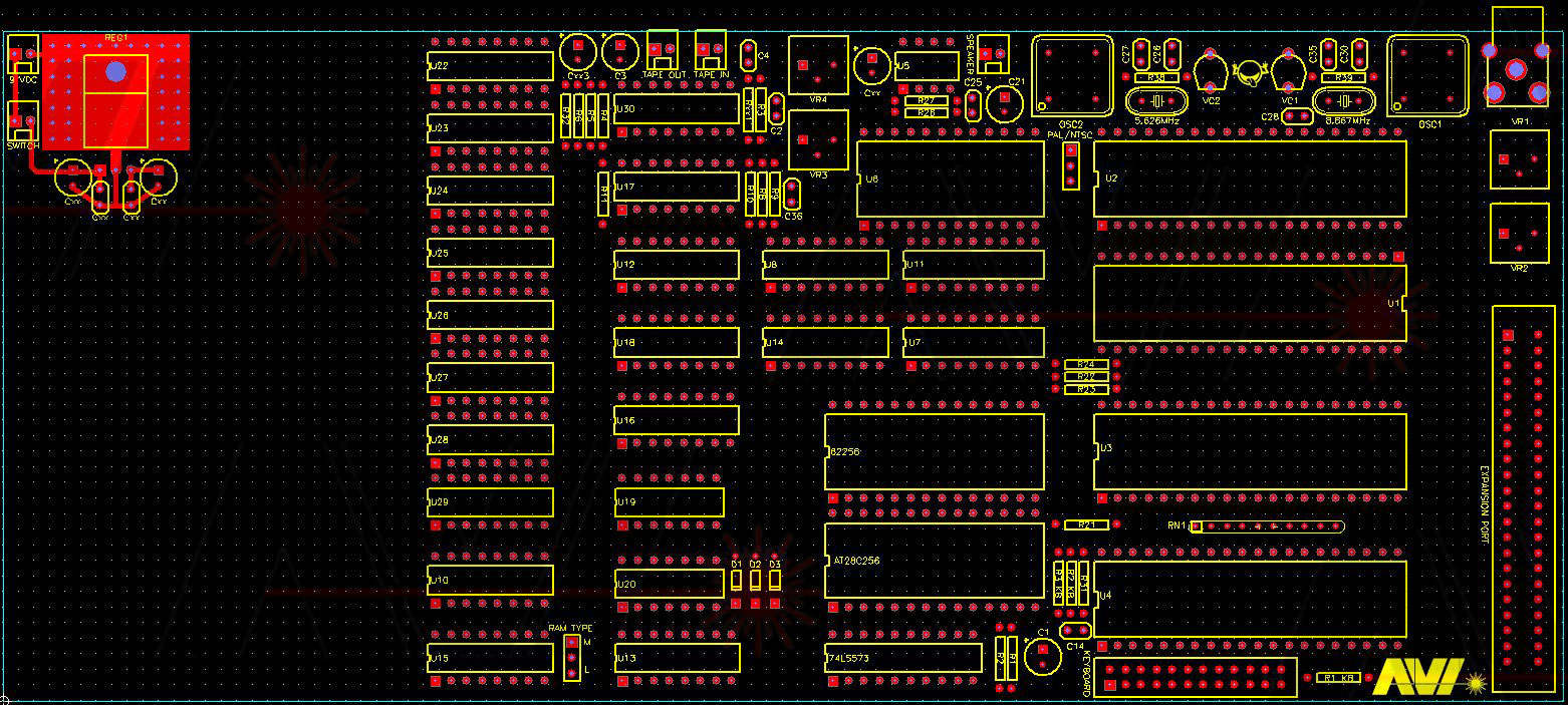
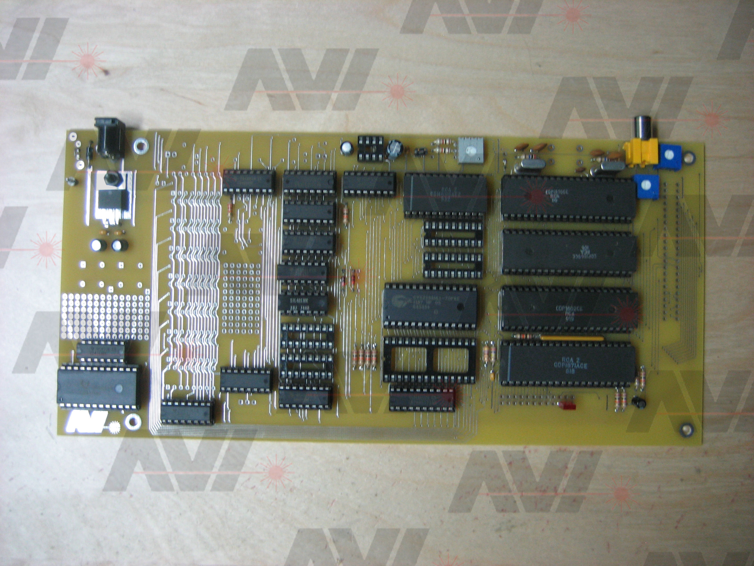
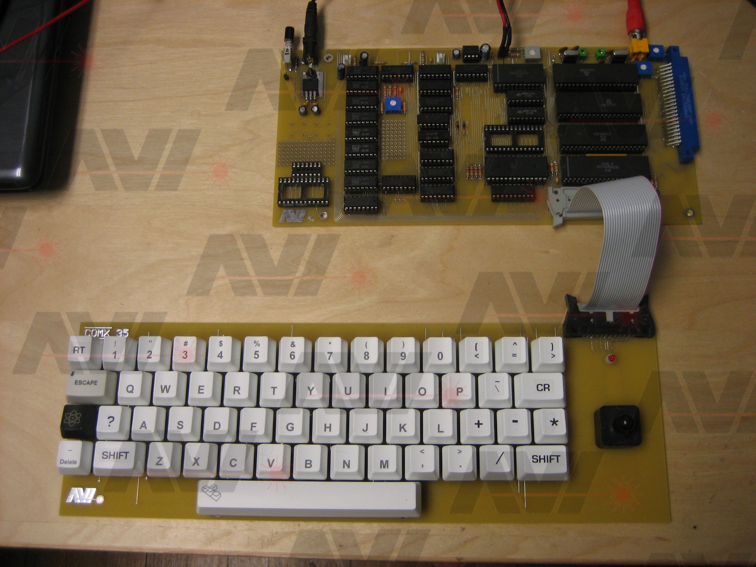
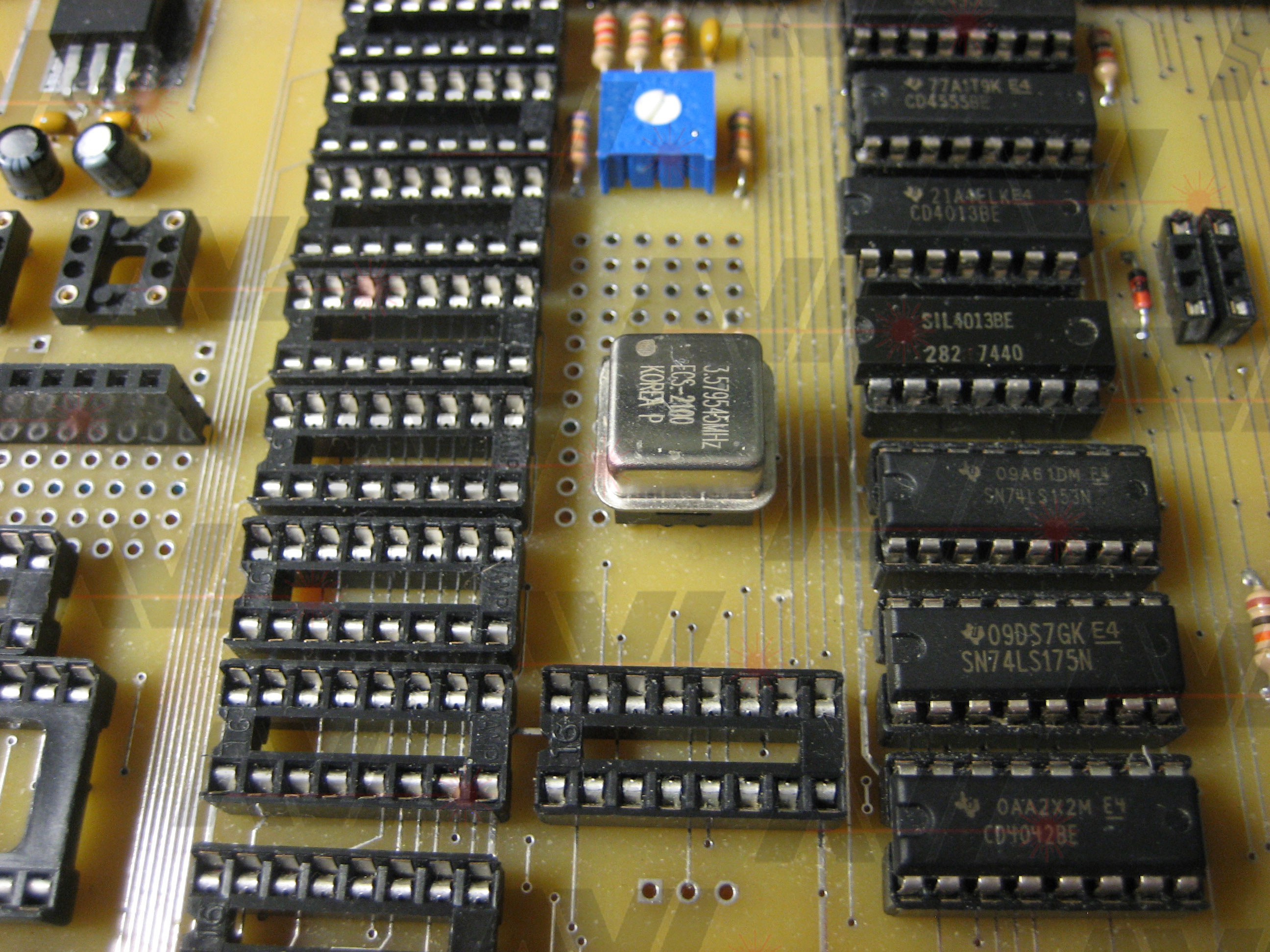
Using the updated schematic I had drawn, I designed a preliminary PCB for the AVI COMX-35.
This is what it looks like:
At this point I placed an order with UTSOURCE (http://www.utsource.net/) for 10 M3723L DRAM chips. I had already collected the rest of the parts.
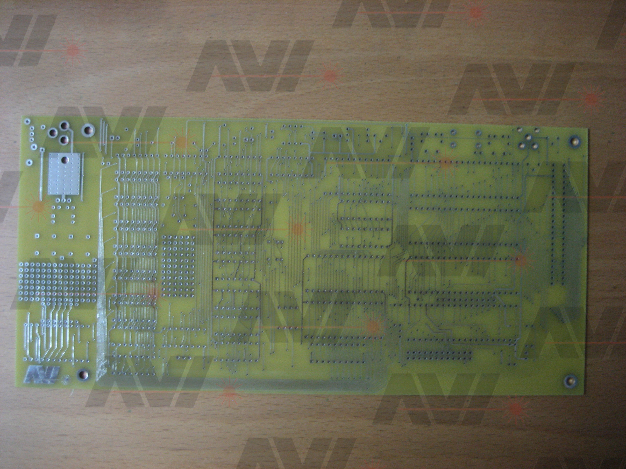
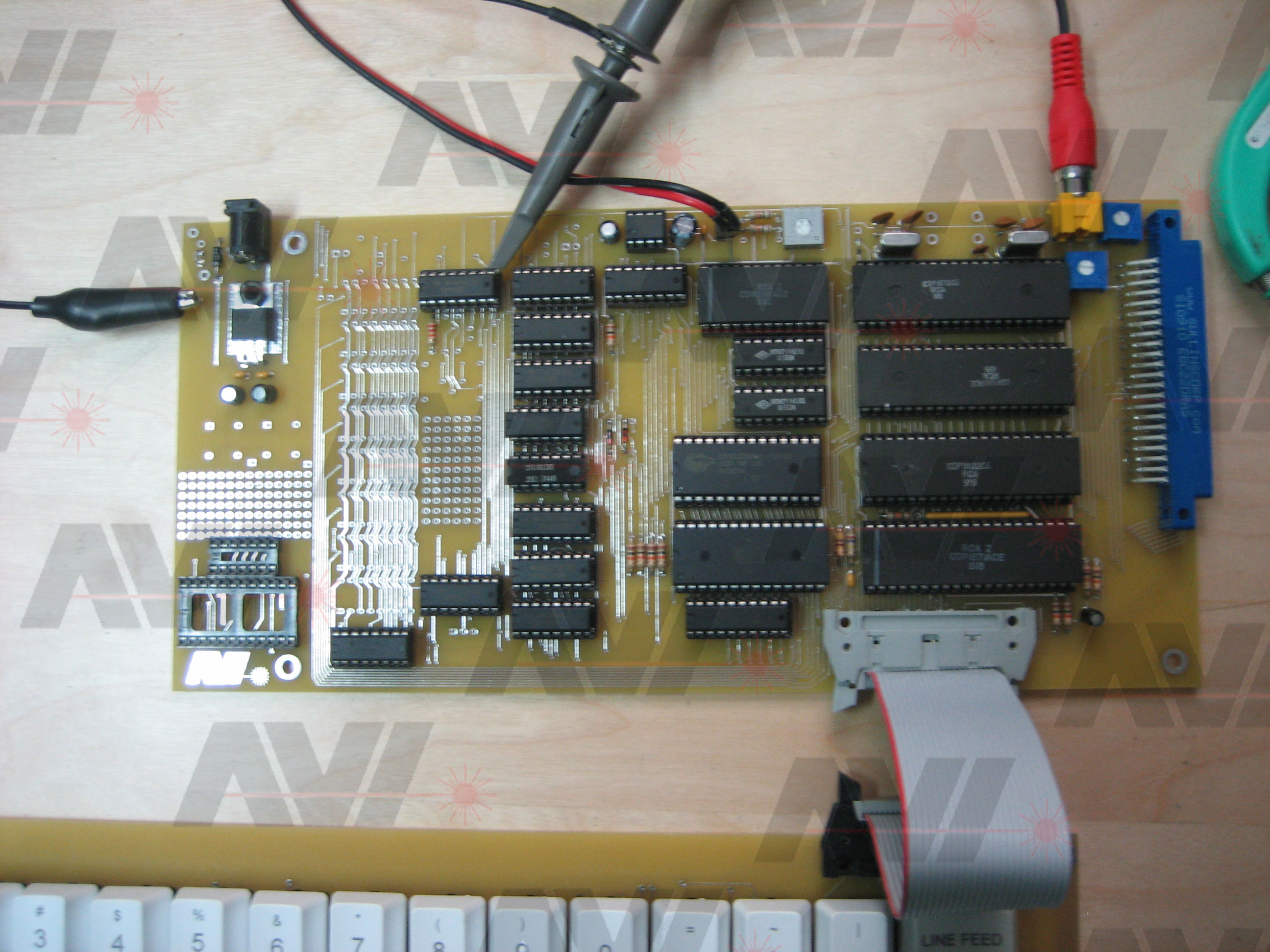
I placed an order to have the board manufactured. Here is the board I received:
Here it is built:
TESTING
While waiting for the dynamic RAM I ordered from Hong Kong to arrive, I installed the Static RAM on the board along with a special address decoder for it. I had a couple minor mistakes, but with those corrected the board was running, but not consistently. Sometimes it would run correctly and others it would just hang or go crazy. Using my oscilloscope I found that I was not getting a good reset signal. I traced around a bit looking for bad solder joints, shorts and the like. Ultimately I found that while building up the board I had forgotten to install a couple of parts, a 120pf capacitor and a 27K resistor in the reset circuit.
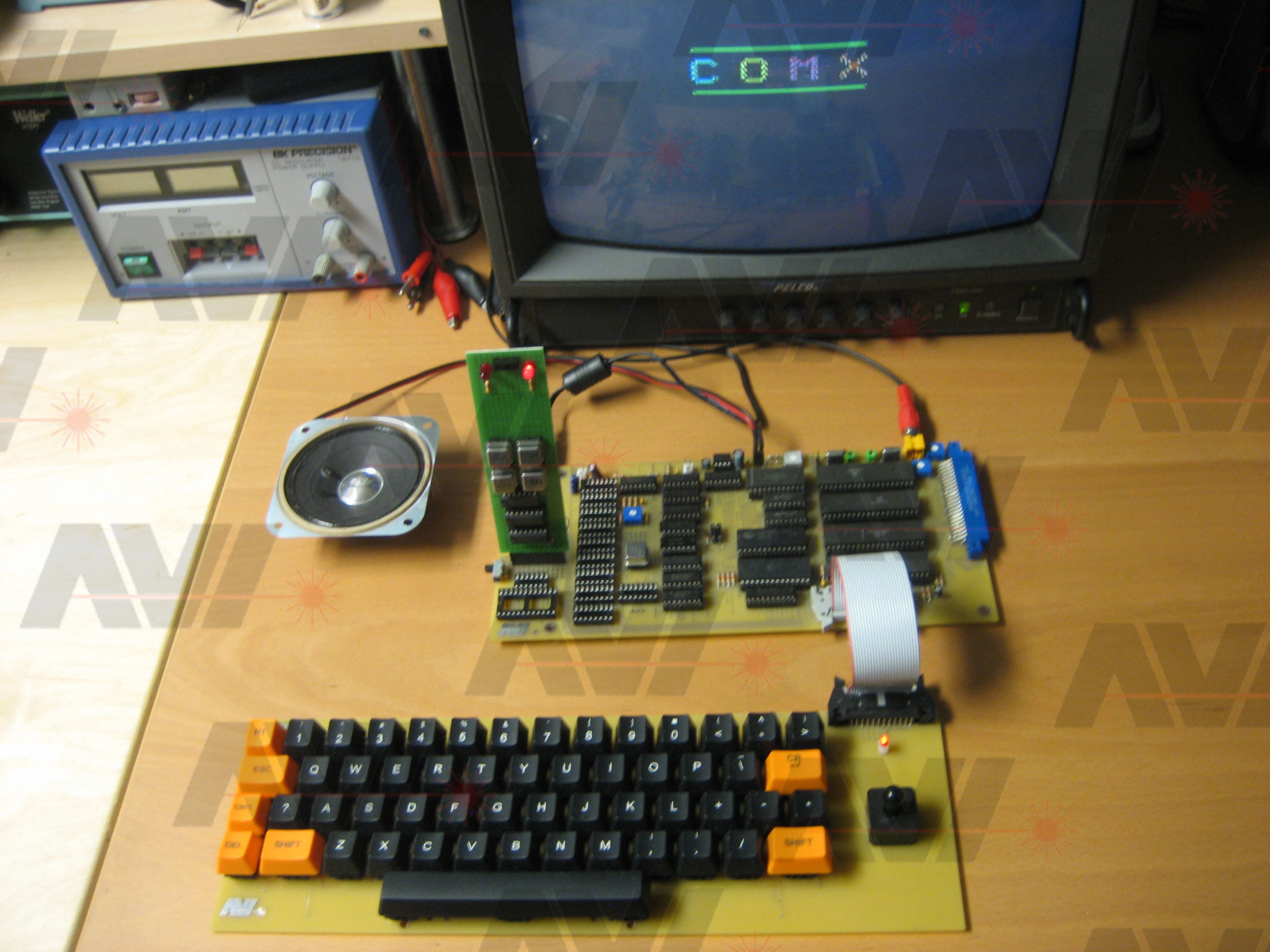
I soldered the parts in and the system began to boot up consistently. The board still has some issues, but I do get the COMX start-up sound (which sounds like "bing-bong-bong") and the COMX logo screen.
 Click to hear the COMX-35 start-up sound.
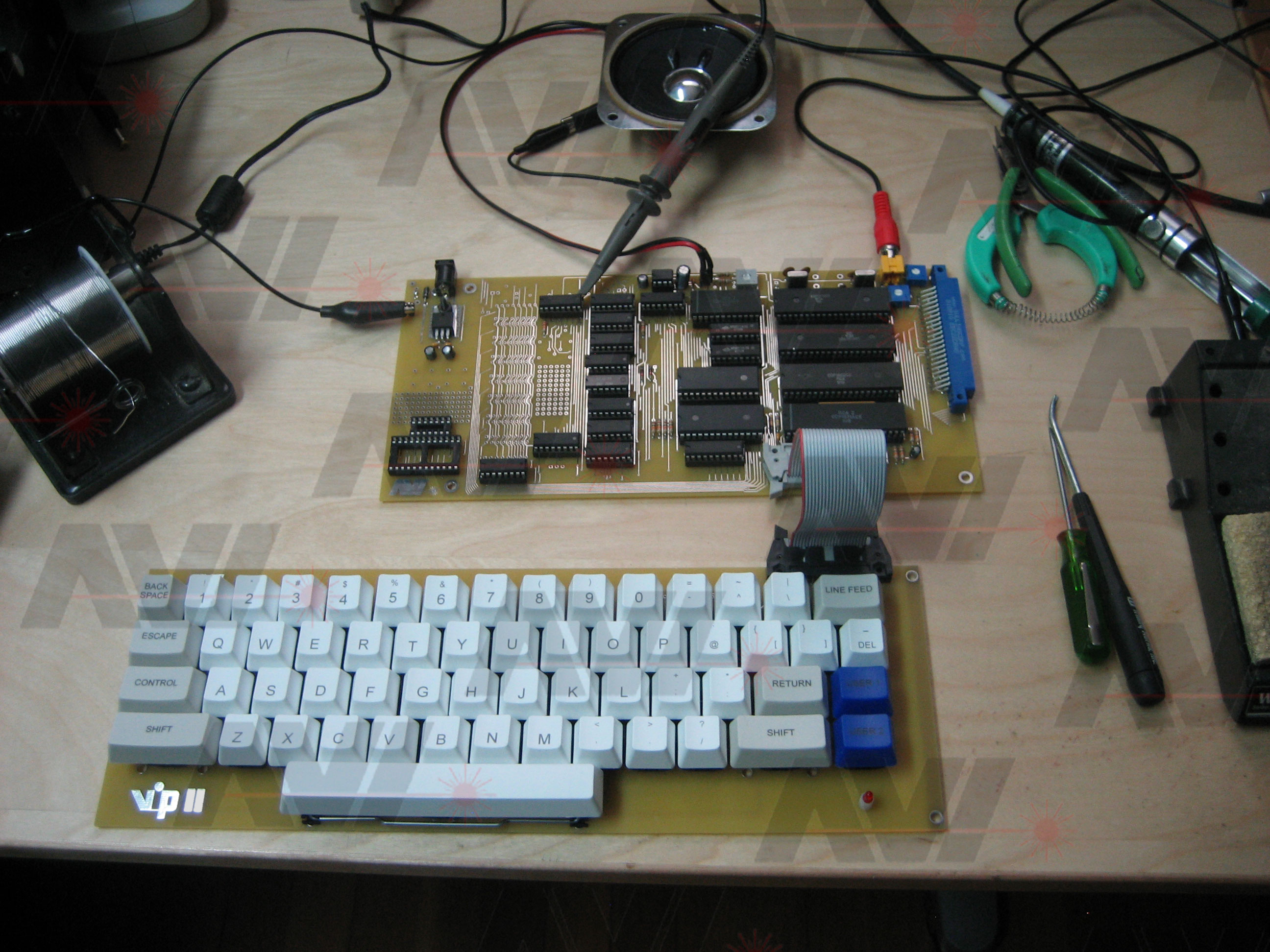
At this point I did not have a keyboard specifically for the COMX built. Since both the VIP II and the COMX-35 use the CDP1871 keyboard encoder, I designed the keyboard connector on the PCB with the same pin-out as the keyboard I built for the VIP II project I did a while back (http://www.cosmacvip.com/VIP2/VIP2.php).
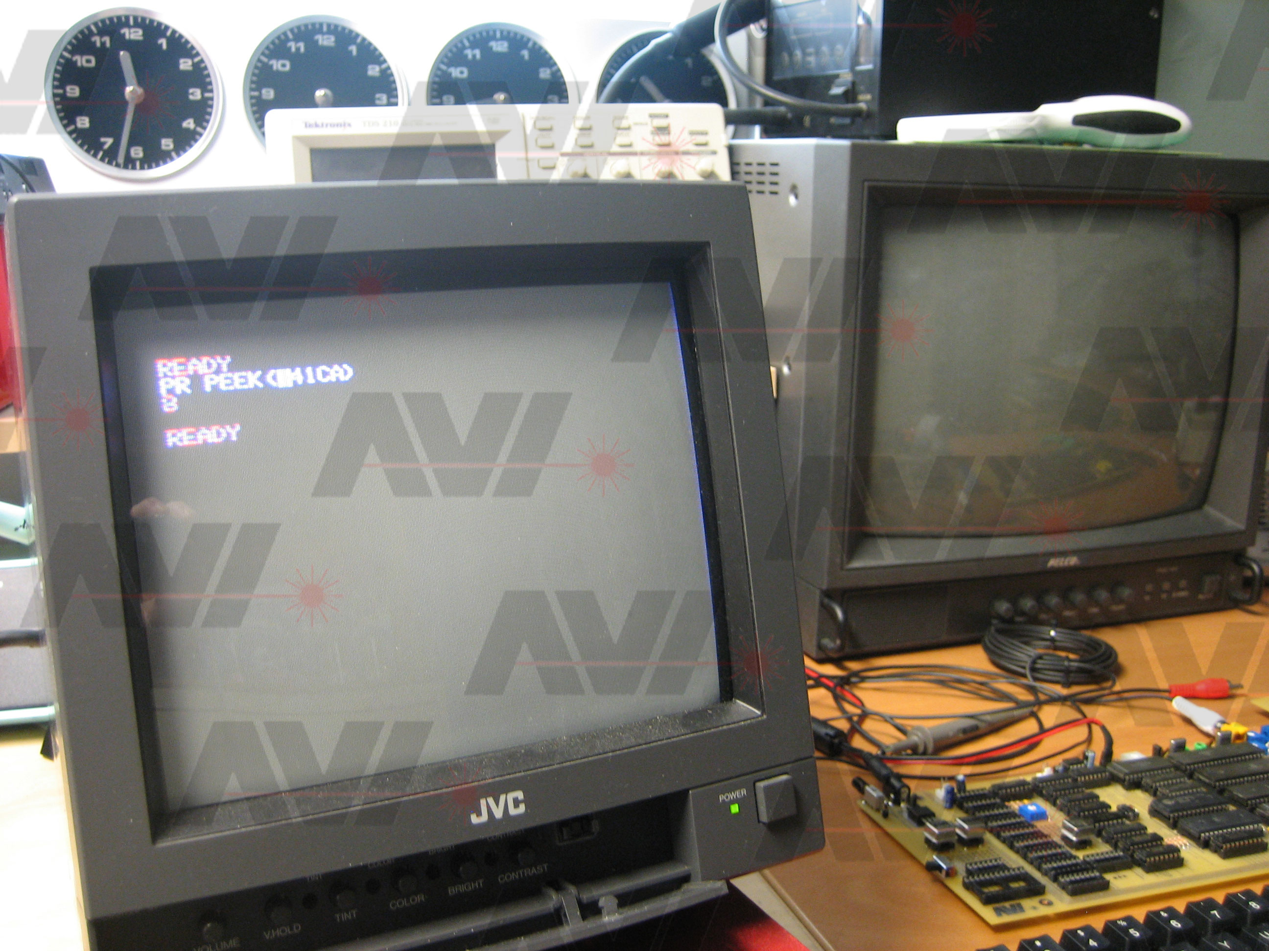
Using the VIP II keyboard I was able to enter text. The keys are mapped differently so the "SPACE BAR" is "CR" and the "DEL" key is space. There are a bunch of differences in the key mapping. However, I was able to get to the COMX V1.0 screen followed by a "READY" prompt.
I tediously entered a few short programs and they all ran fine. I did a "PEEK(@41CA)" and was able to confirm that the board thinks it is a PAL COMX (I got a 9 back from the peek). You can read more about the mode selection here, on page 135:
http://www.comxclub.hobby-site.com/IntroductionintoBasicProgramming.pdfMORE TESTING
I had the board working pretty well at this point, but it still does not always work with the Super Board (/superboard.html). It responds like there is a memory conflict. When the Super Board is installed, I get some new, weird errors. Sometimes it runs and sometimes it fails.
This was a tricky problem to track down. To make a long story short, I had a problem with address lines A13 and A14. I am using a 32K EEPROM for the onboard system ROM. This ROM only needs to be 16K. I cut address line A14 so it would not reach the ROM. I then grounded the A14 line on the ROM. The board became more stable, until I tried to enter and run a Basic program. When I cut A14 from the ROM, I did not put a jumper around the grounded A14 ROM pin to the Static RAM. The RAM's A14 line was also grounded. This caused the RAM to appear to be 16K. This seemed to cause a problem with COMX Basic.
I made another cut disconnecting the A14 line between the ROM and RAM and then added a wire from the A14 line directly to the RAM. Now the system was working and running pretty stable.
TESTING WITH SUPER BOARD
With the main board working pretty well, I installed the Super Board (/superboard.html) in the expansion connector on the main board. It did not work. There was something wrong with the external ROM disable (/EXTROM) circuit. If I removed the ROM from the COMX itself I could get the SB to boot. I did get the three line start-up message from the SB once. Most times the system fails to boot with the SB installed.
Since it seemed to be a memory conflict, I watched the chip select lines on both the internal and external system ROMs and noticed that they were both being activated at the same time. This should not happen and will cause data bus contention, which would manifest itself in the sort of intermittent problem I was seeing.
It turns out I had forgotten to install a 22K pull up resistor on the board. When I soldered this part in place the Super Board now worked with the AVI COMX-35.
EXPANSION BOARD TESTING
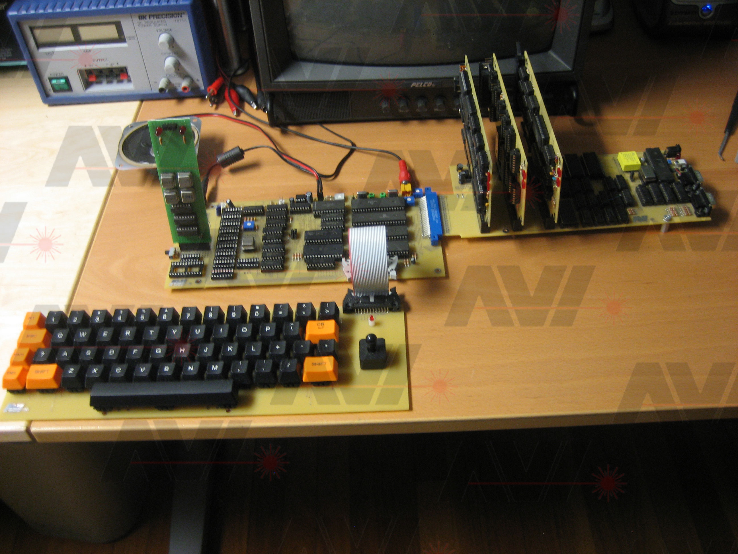
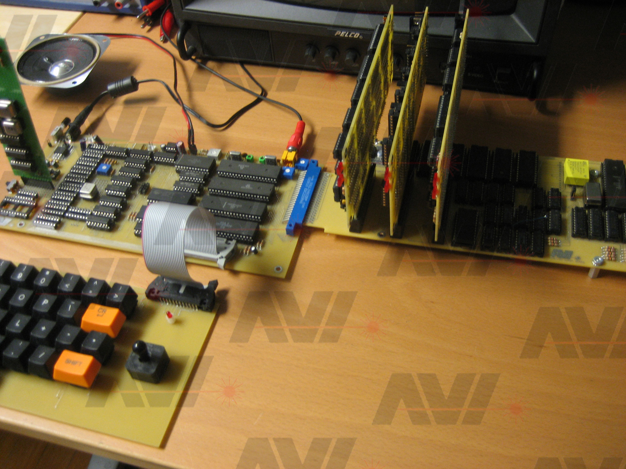
With the system now working with the Super Board, it was time to see if expansion boards would work. This is where things started to not make sense. If I installed the printer card into the Super Board, the COMX would run for a few seconds and then go berserk.
If I installed the printer card into the COMX directly, it worked fine. I did everything it should. So I installed just the Super Board in the COMX and ran it through its functions. Once again, everything worked as it should.
It made no sense to me. Individually they worked fine, but together they would fail after a few seconds.
As a test, I installed the printer card into the Super Board again. I powered up the system and issued a 'USB MON' command. This launches the F&M Monitor (http://www.emma02.hobby-site.com/comx_fandm.htm) that is built into the Super Board. I set it to look at the location of the ROM on the printer card to see if there would be an issue. The display showed a normal dump of the printer ROM with no cable attached.
After a few seconds the system would go crazy. I was stumped.
COMMENTARY
When I was younger, anytime a circuit failed to work I immediately decided that "The Chip Is Bad" (TCIB). As I gained more experience I found that most likely the problem was human error (Me):
- Chip installed backwards
- Loose wire
- Bad solder joint
- Bad or incorrect design
Or as I have shown above, forgetting to install a required part.
In just about every incident, the chip was not bad.
As time went on, I started looking for the most likely cause when problems arose. I used the same thought process with the COMX I built. I figured I must have:
- Incorrectly "Beeped" something
- Drew the schematic incorrectly
- Didn't follow the schematic when laying out the PCB
- Missed a connection while researching the COMX
- Installed the wrong part
Along with that, my COMX worked fine by itself. It worked fine with the SB attached. Only when one of the expansion boards was plugged in did a problem occur. Since everything seemed to work, and for the reasons I just listed, it never crossed my mind that the 1802 itself had a problem.
I made a chart of all the pins used by each of the boards in question (Super Board, Printer and Floppy), isolated the pins they didn't have in common and did exhaustive testing on them.
I was so convinced that I missed a single connection that I rechecked the board against my schematic, and then my schematic against the board again. I was positive I had drawn the schematic correctly. I had nothing else to look for.
I decided to leave the board alone for a few days just to clear my mind.
ENTER THE FLUKE
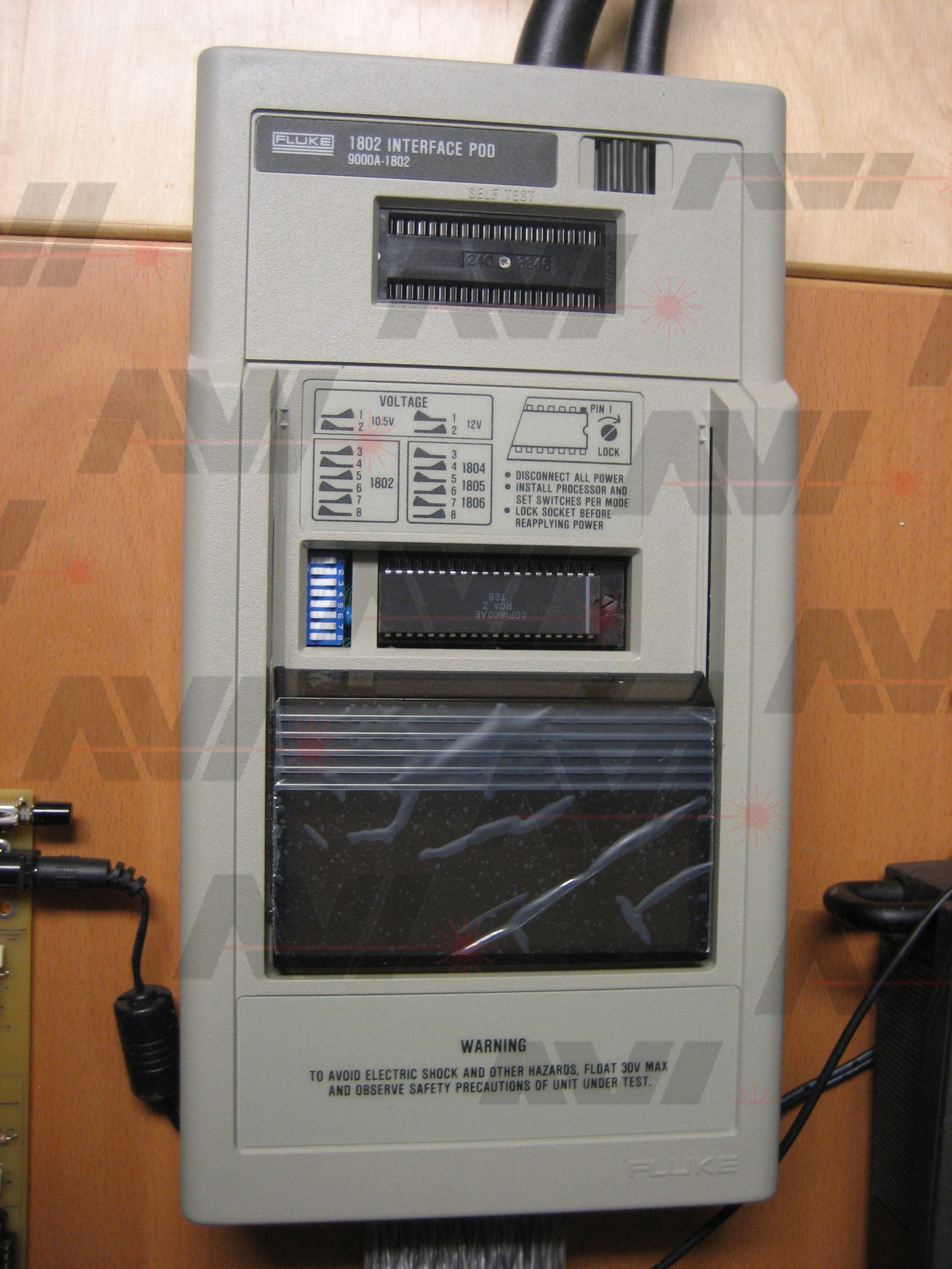
I had recently purchased a used "Fluke 9010A - Micro-System Trouble shooter". I was also lucky enough to find a good deal on, what turned out to be a brand new, 1802 POD for it. It was new old stock that was manufactured in 1989.
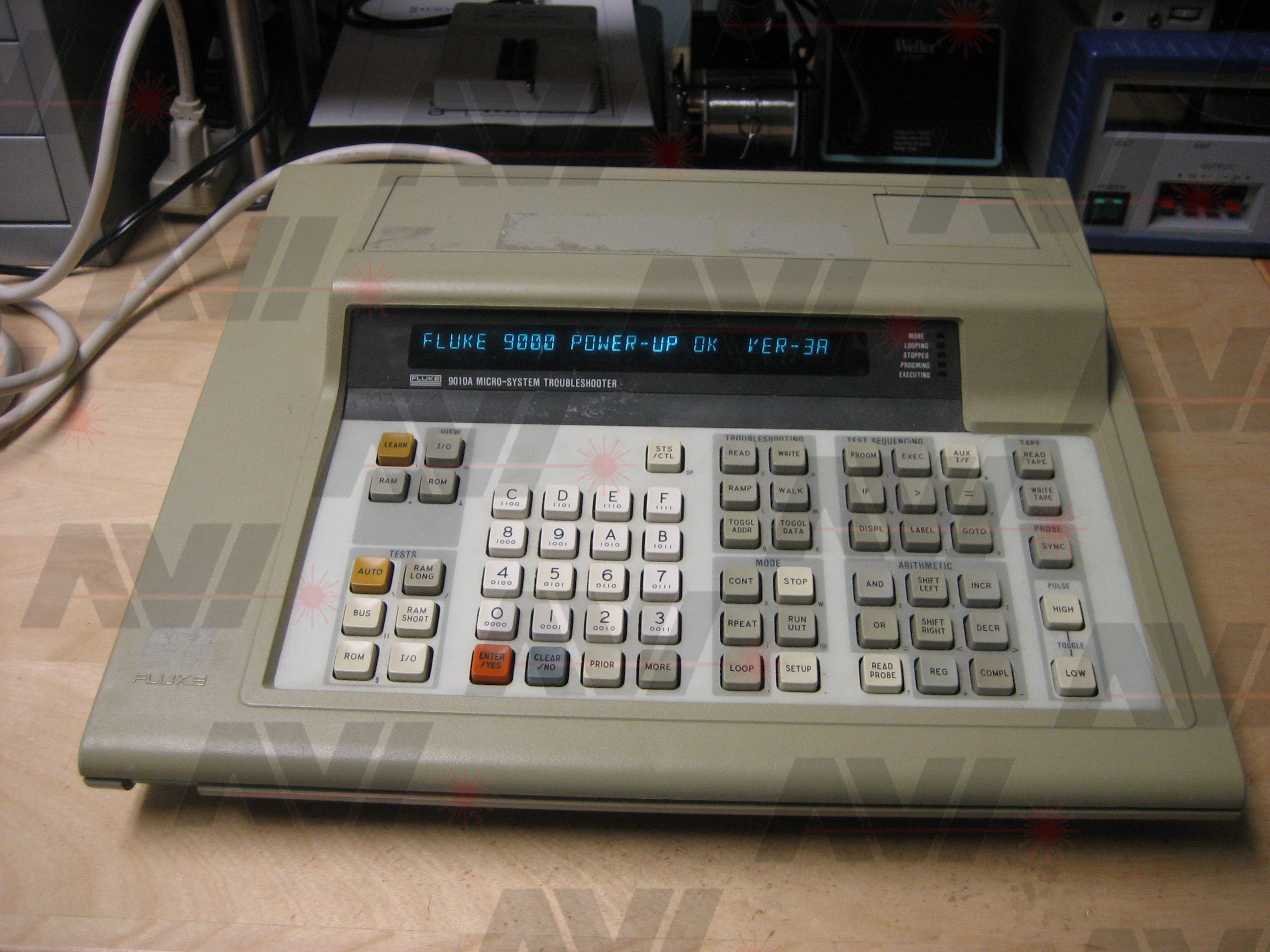
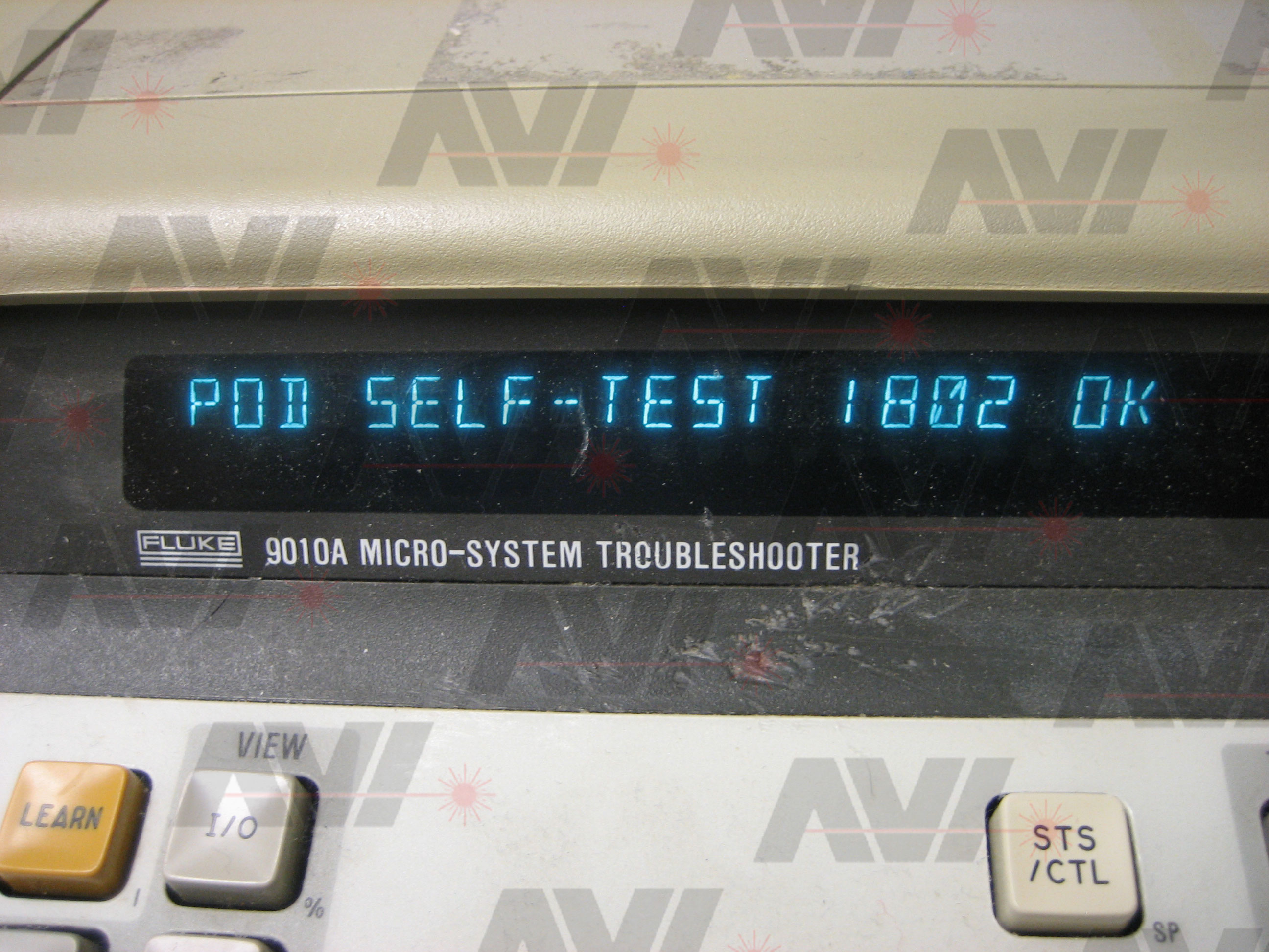
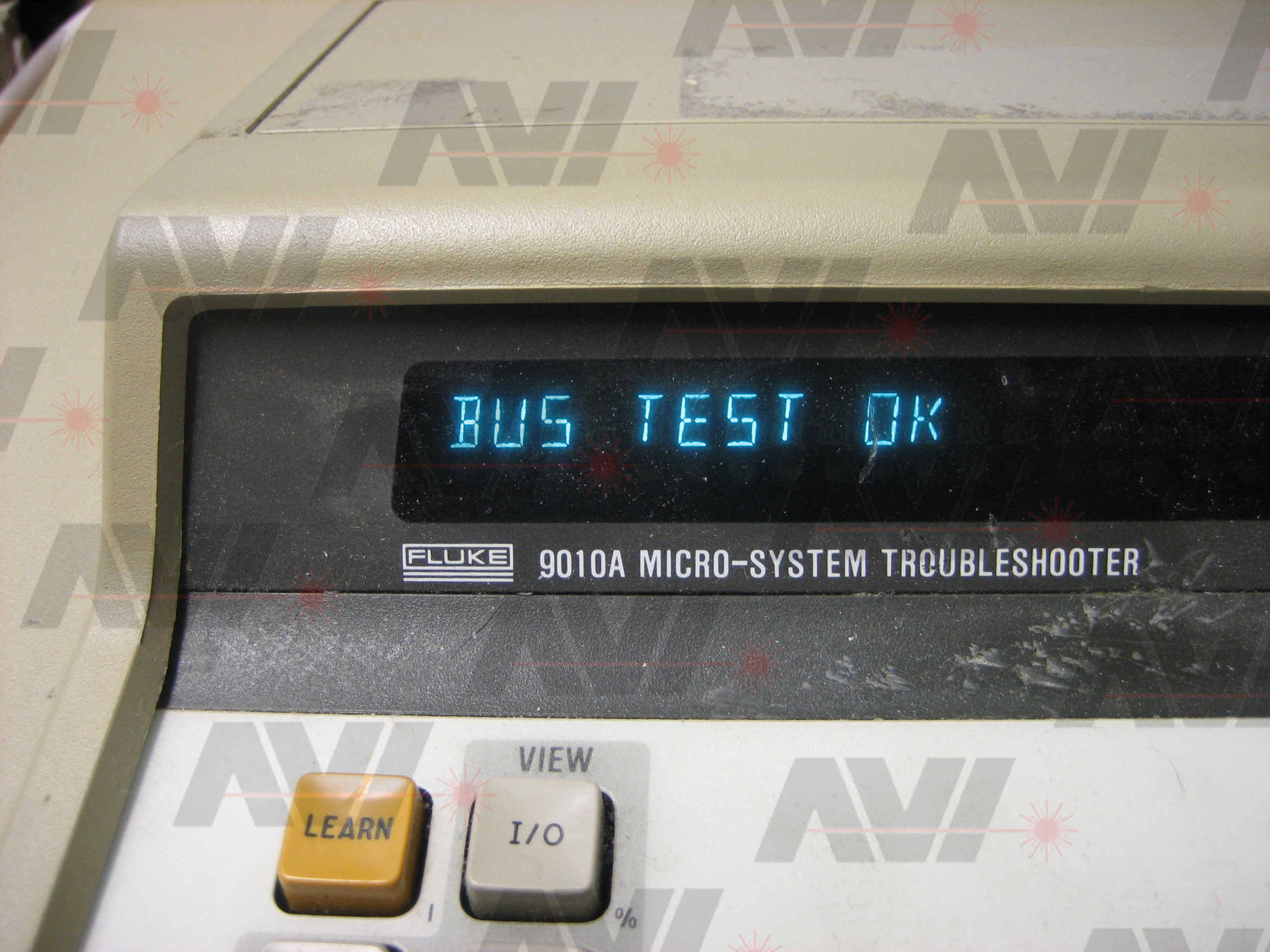
When the pod is connected to the Fluke 9010A and the "AUTO" key is pressed, a self-test of the pod is performed.
This would be a good chance to put it to use. I decided to give it a try on my COMX and see if it could see any problems. The POD works by being installed into the socket of the 1802 of the target system. In this case the 1802 on my COMX.
I was able to check that the 1802 Data and Address busses both worked, and had no shorts. Both checked out fine.
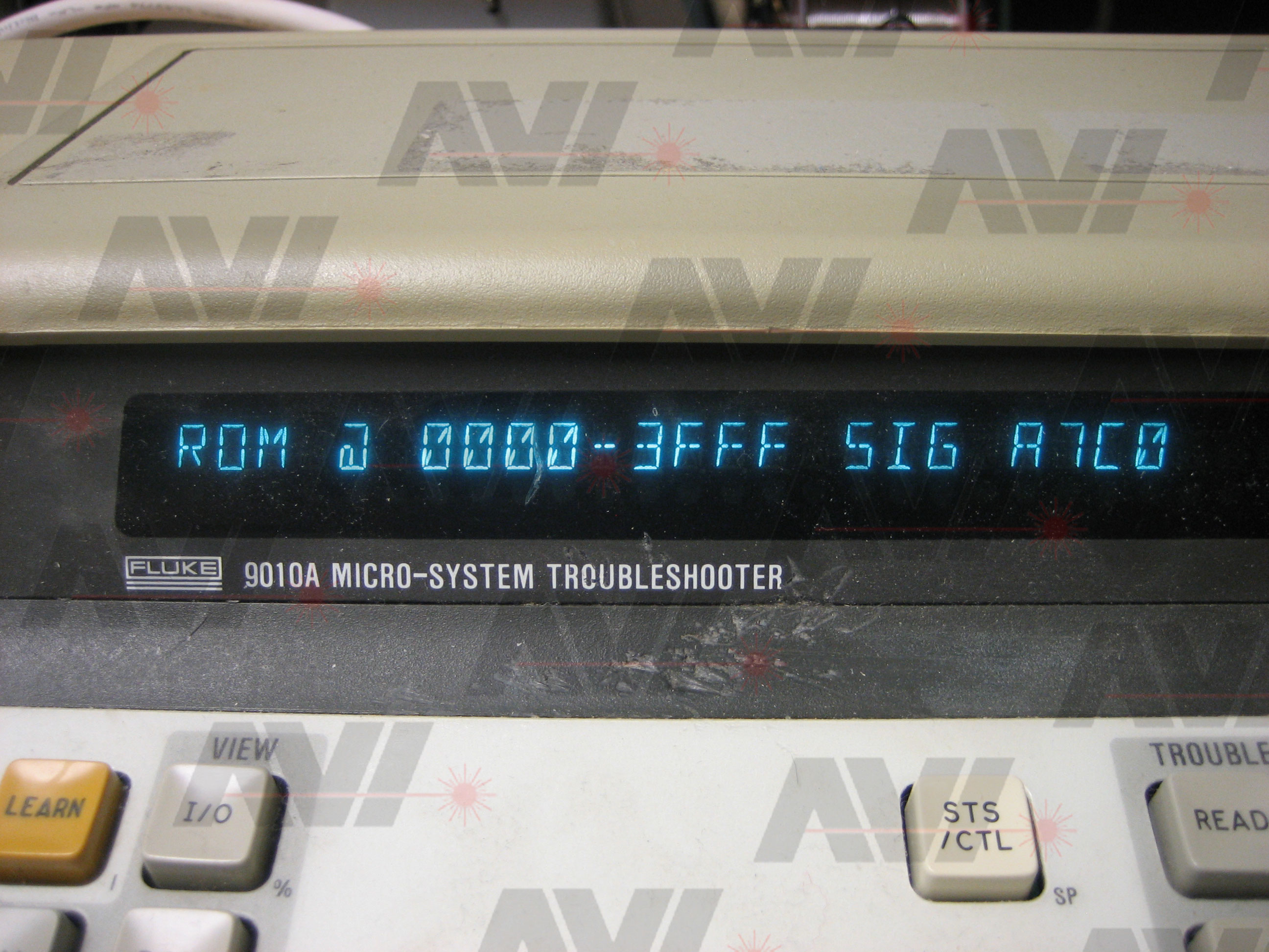
The Fluke can analyze the memory map of the target system. By pressing the "LEARN" button and entering a start and end address to check, the fluke scans all the addresses in the specified range and finds all areas of RAM and ROM. The image below show the Fluke currently testing memory at 0200h to 02FFh.
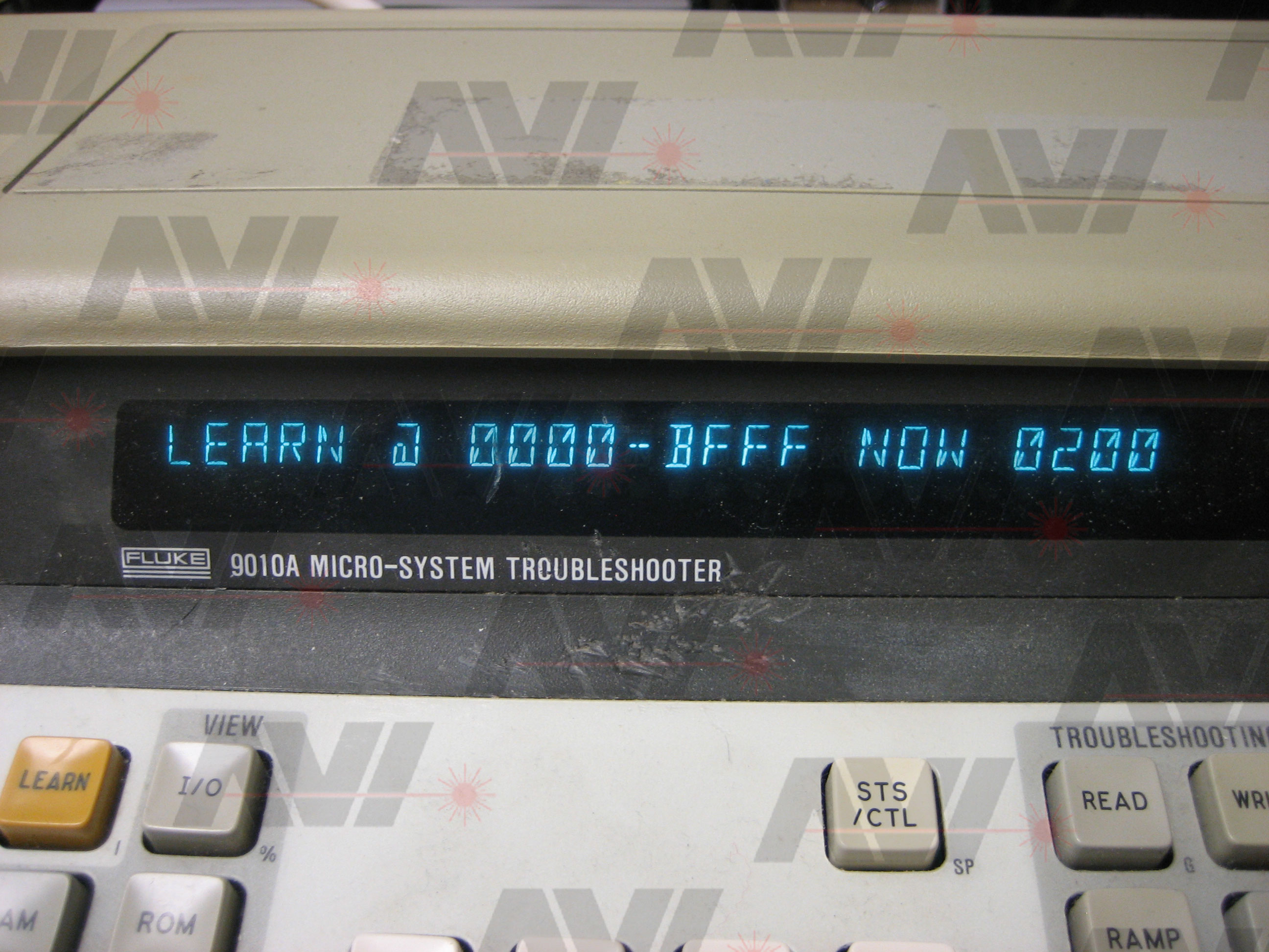
When the scan is done "OK" is displayed.
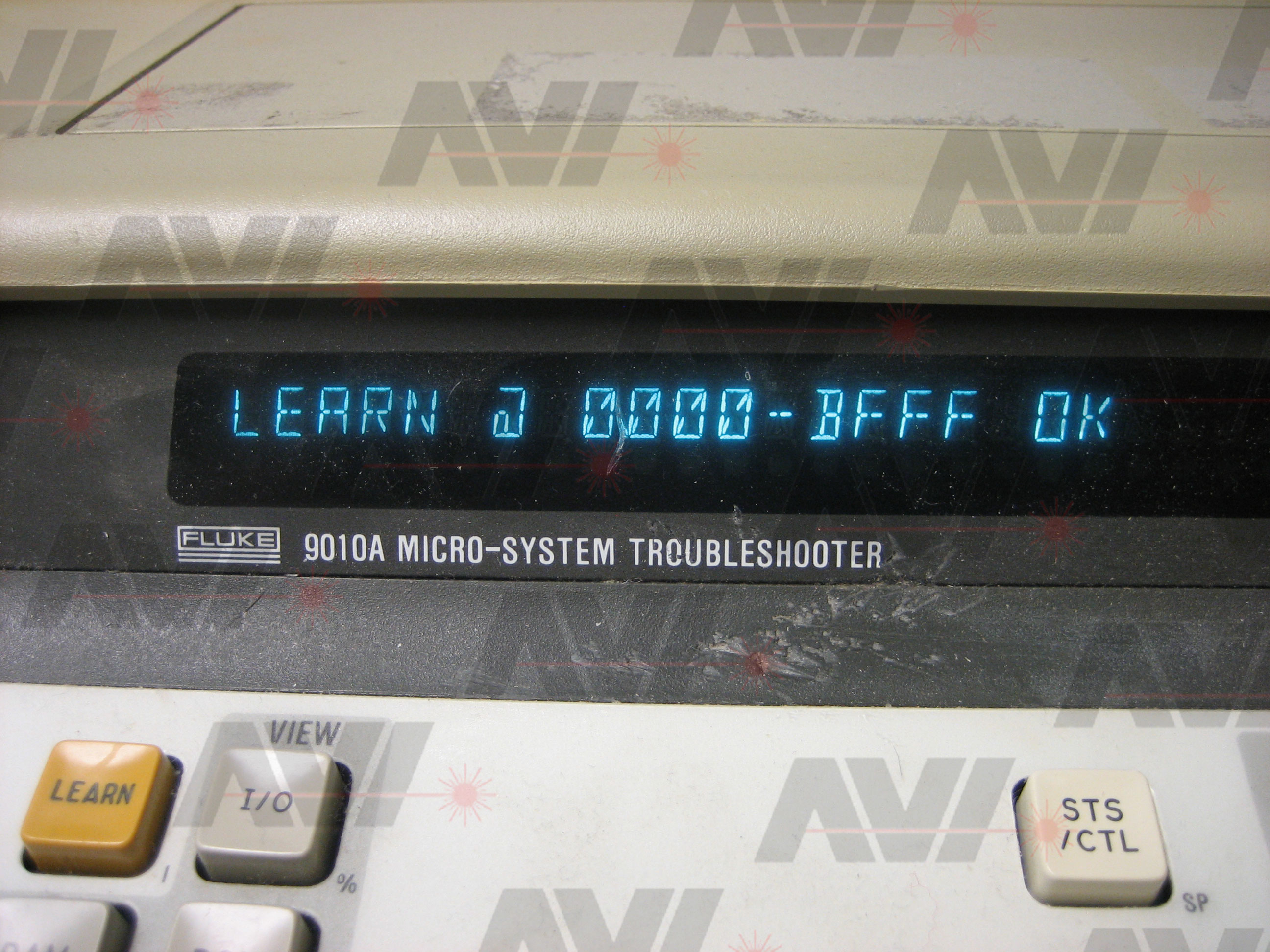
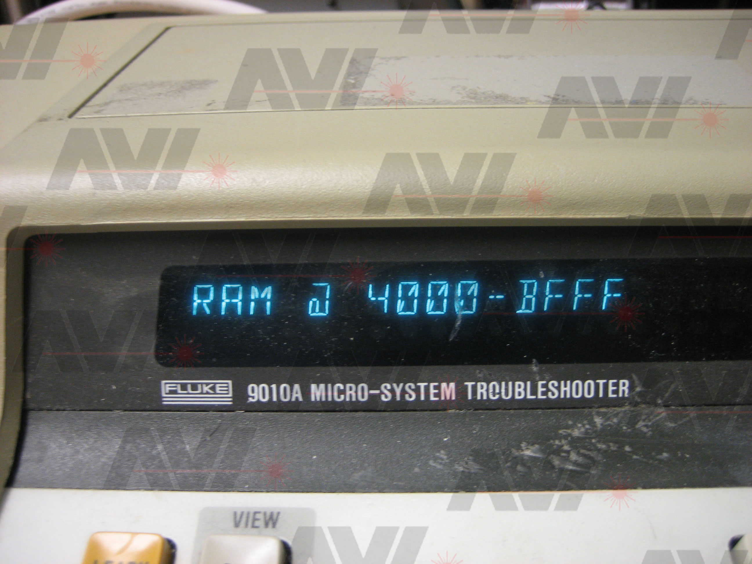
By pressing the "RAM" and "ROM" buttons on the Fluke, the addresses where each is found can be displayed.
I was able to check that all locations in the RAM worked, which they did. The Fluke 9010A uses a ROM signature, which is sort of like a checksum, to check that a ROM is okay. Using a tool I found online, I was able to create a checksum for the AVI COMX-35 ROM. The Fluke indicated that it saw the ROM and that it was also okay. I also checked other random 1802 signals.
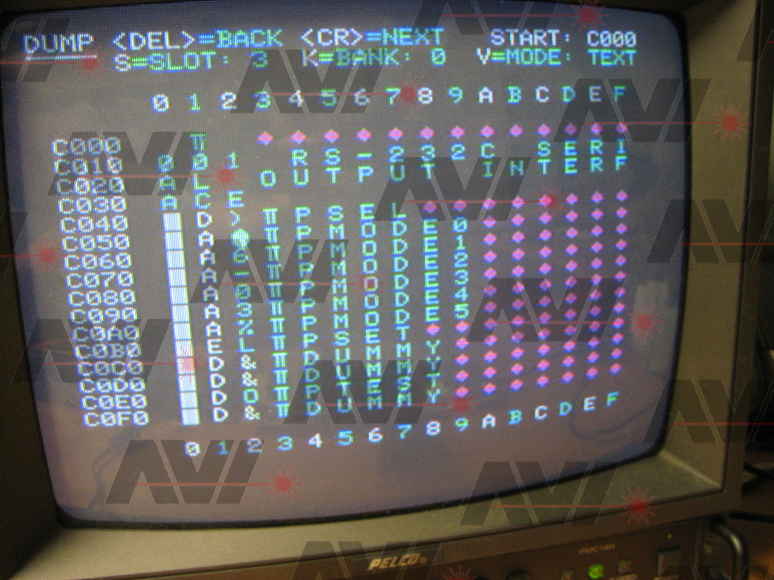
With all that tested, I finally pressed the "RUN UUT" button (RUN Unit Under Test) with a starting address of 0000h. The COMX start-up sound played and the logo came up. I pressed a key and was presented with the COMX copyright and a "READY" prompt. I powered down and installed the printer card with no cable installed (printer card in serial mode). I re-issued the "RUN UUT" using 0000h as the starting address. I got the start-up sound and logo again. Pressed a key and got to the "READY" prompt again. I have been able to get to this point all along. Only when I accessed the card did I have trouble.
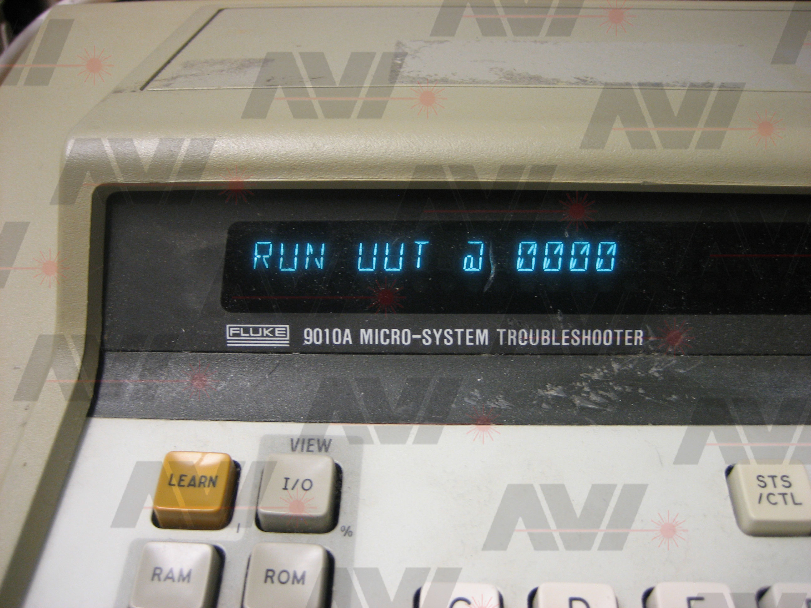
I let the system just run for over a minute without crashing. I then typed 'CALL(@C0B0)' and pressed enter, this should start the routine that sets the serial communications parameters.
I expected the COMX to crash. I was surprised to see this displayed:
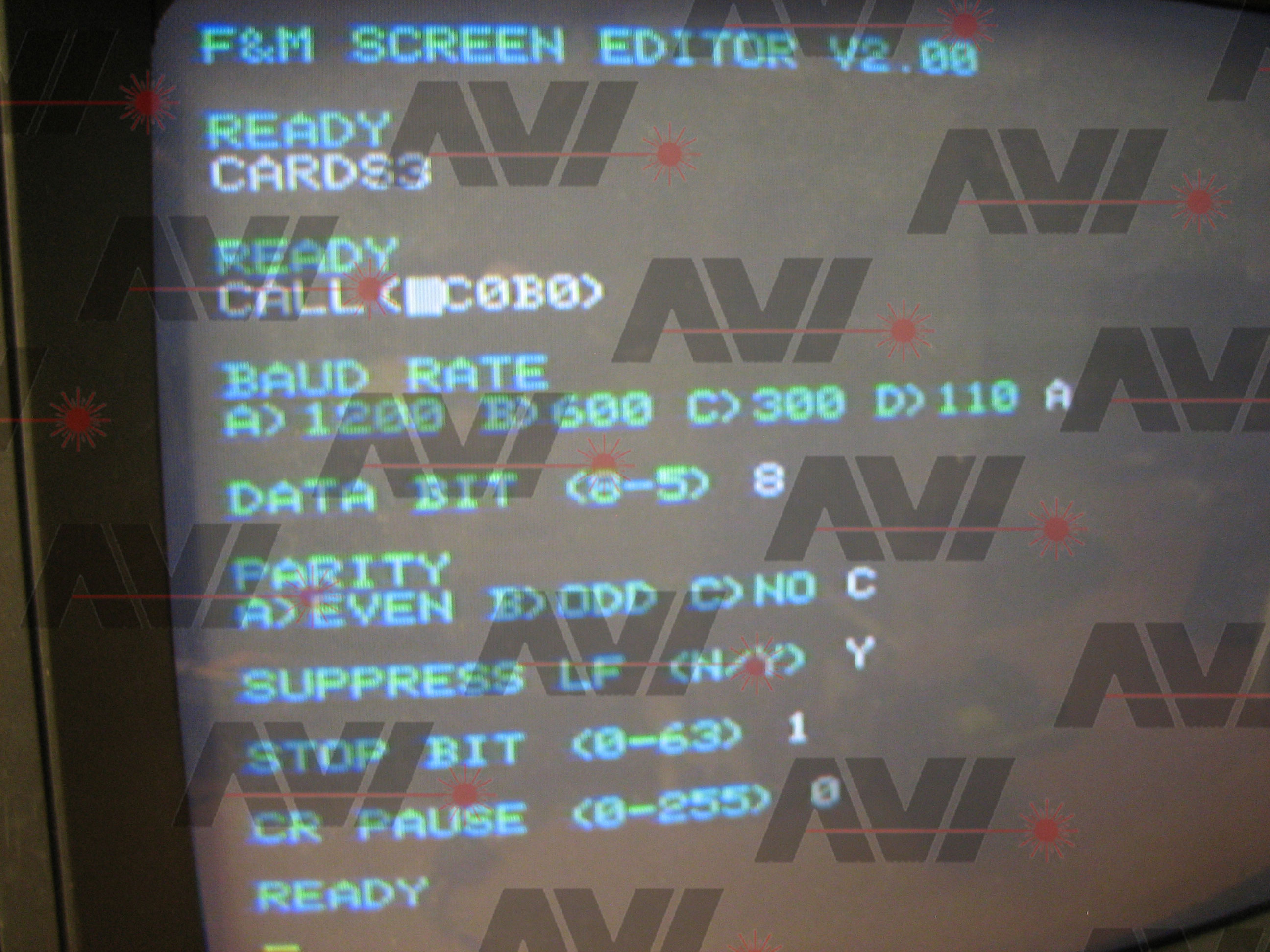
I had not done anything else to get it to work this far. So I entered 'USB MON' and was presented with the built in F&M Monitor, as it should when working correctly. I immediately thought I must have had a bad solder joint or other connection, so I carefully removed the POD and re-installed the original 1802.
I powered up and worked my way to the point where I typed 'CALL(@C0B0)' and pressed 'CR'. The COMX crashed.
I reinstalled the POD and tried the "RUN UUT" again. With the POD installed the COMX worked as it should with no crash. I powered down and installed the SB with the printer card installed on it. I tried the "RUN UUT" again and everything was working. I added the floppy card and drive and tried again. Everything worked. The only difference was the POD replacing the 1802.
I had no choice but to try a different chip. After removing the POD, I installed a different 1802. I still had the SB inserted into the COMX with the printer and floppy installed into the SB. I cycled power and everything worked!
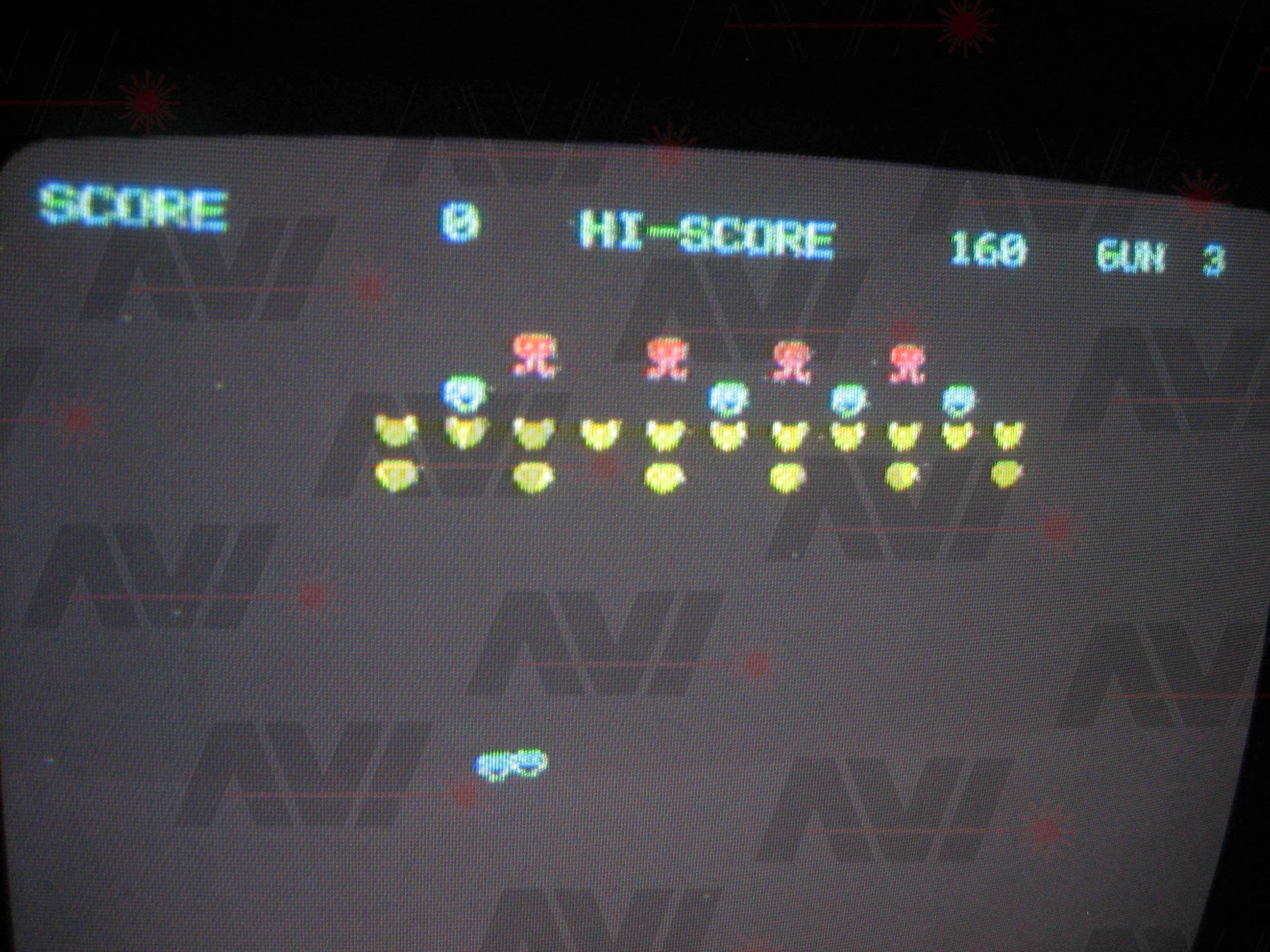
It is quite frustrating to have spent that much time looking for a problem that was right there, but like I said, I had no reason to suspect the 1802 was bad. I let my COMX run for over 10 hours, periodically trying different things. I also did some "testing" of the system by playing a few of the games built into the Super Board: 'USB TENNIS' (like Pong), 'USB SPACE' (like galaxians) and 'USB WORM' (a cool version of snake). I had no trouble with the system, it ran fine.
DYNAMIC RAM
I received the Dynamic RAM I ordered from Hong Kong, so I installed it. As I described above, my address decoder was missing signals required by the DRAM, so I removed the chips in my circuit and reinstalled the chips from the original COMX-35 circuit. The Dynamic RAM worked fine. I asked Marcel if he had, or knew of, a memory test program for the COMX. He did not have one. Marcel wrote me a short program to test the internal RAM. The memory tester worked great. It indicated that all the Dynamic RAM was working.
With the DRAM working, the only thing left was to put together a COMX-35 specific keyboard.
KEYBOARD
Using the VIP II keyboard became a real hassle so I designed a keyboard specifically for the AVI COMX-35.
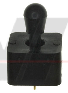
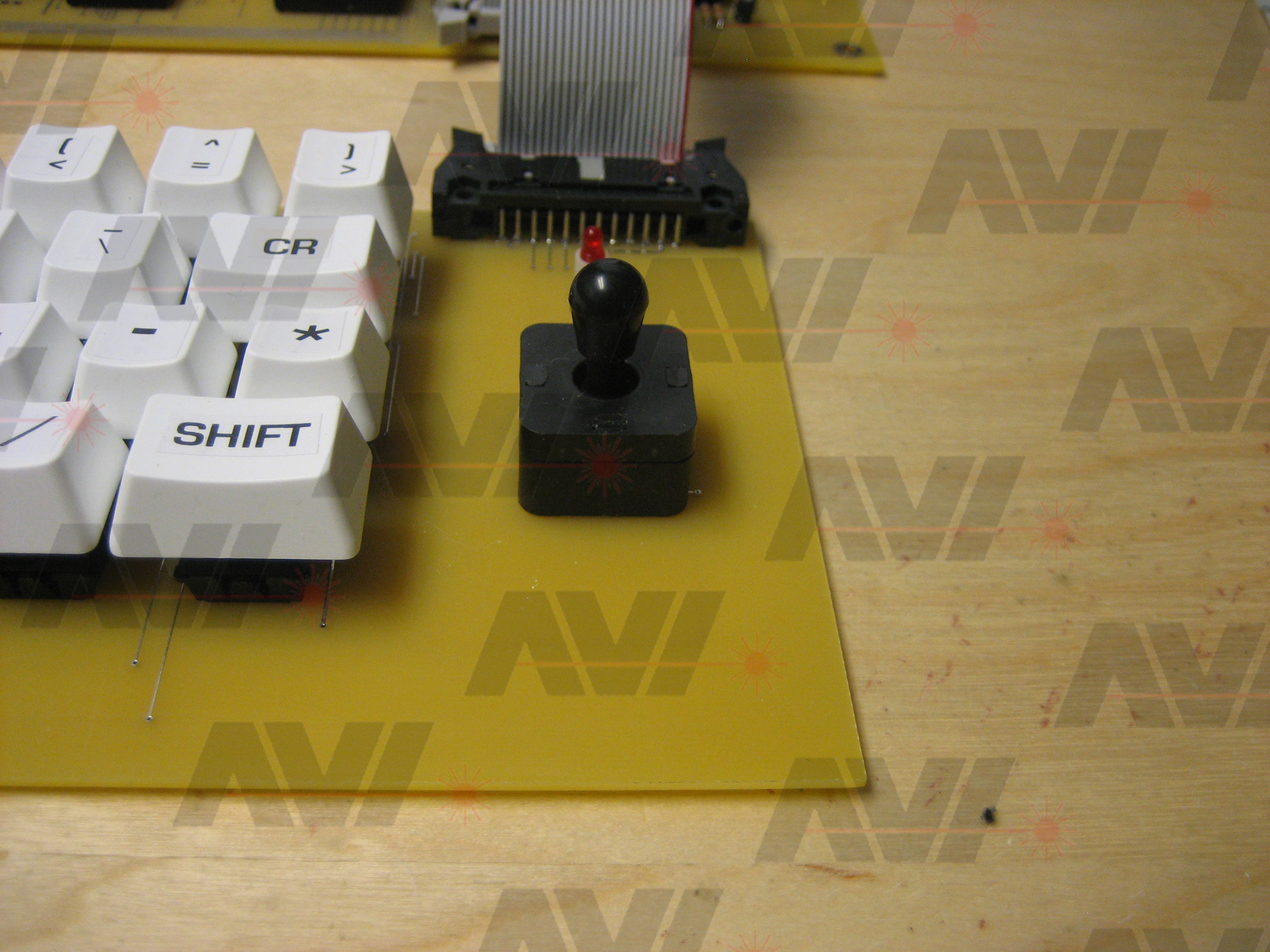
The first thing I needed to find was a small board level joystick. I found a couple but settled on a Grayhill, Inc. GH7455-ND (http://www.digikey.com/product-detail/en/04A-B01/GH7455-ND/2138044):
For the keys themselves, I used Cherry MX Blue switches. These were the same ones I used on the VIP II, so I had a bunch of them.
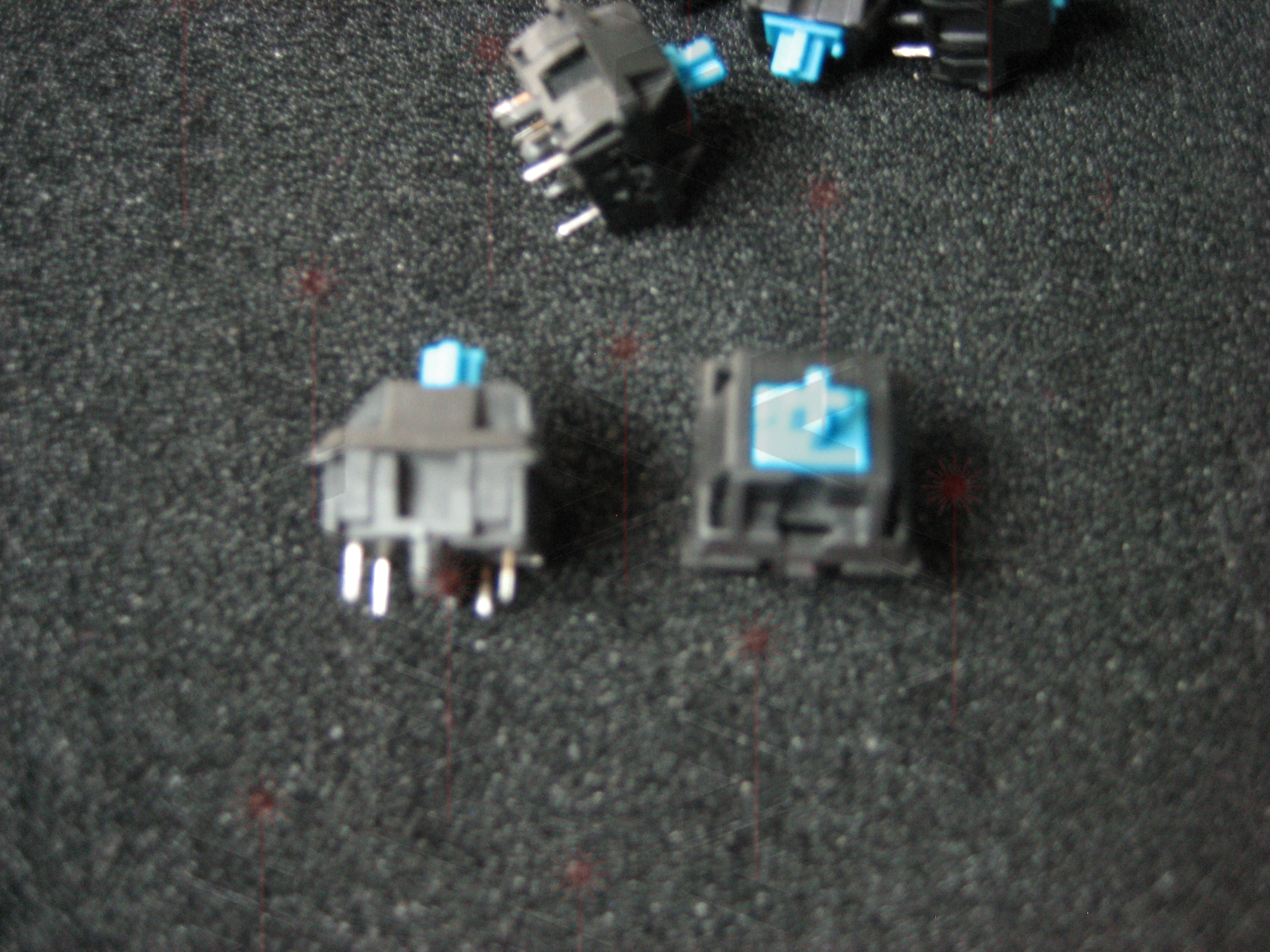
I used switches I had on hand, left over from the VIP II project.
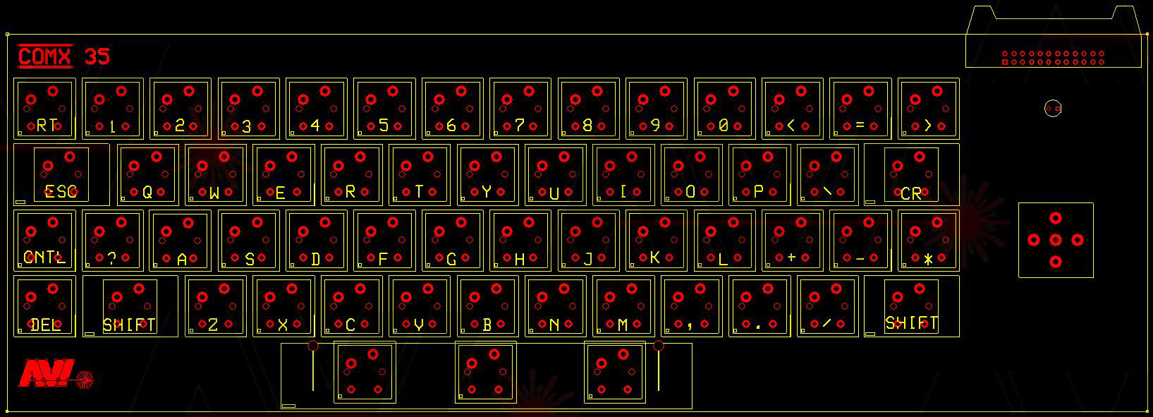
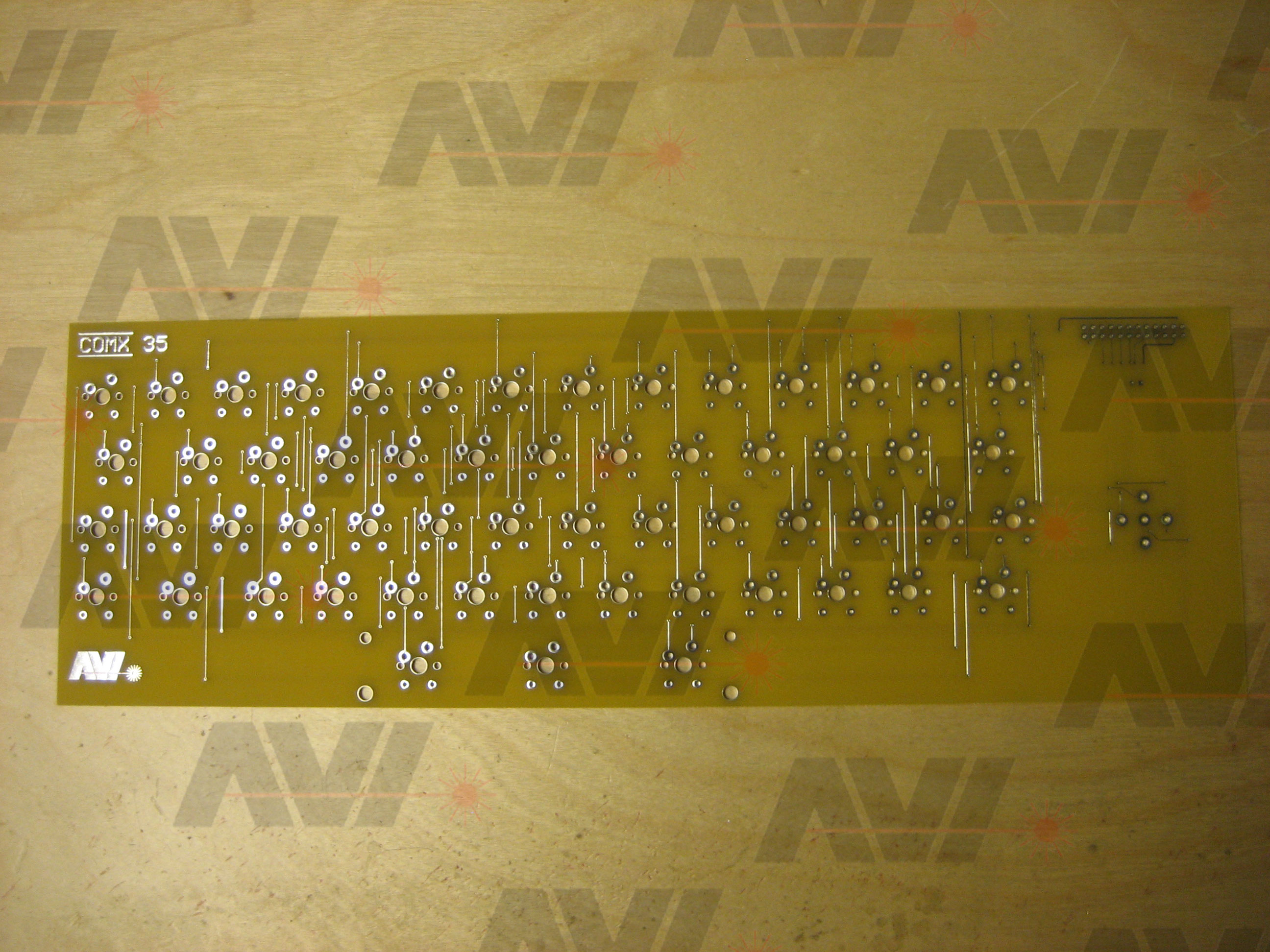
I laid out a PCB for the keyboard including the joystick. Here is what I came up with:
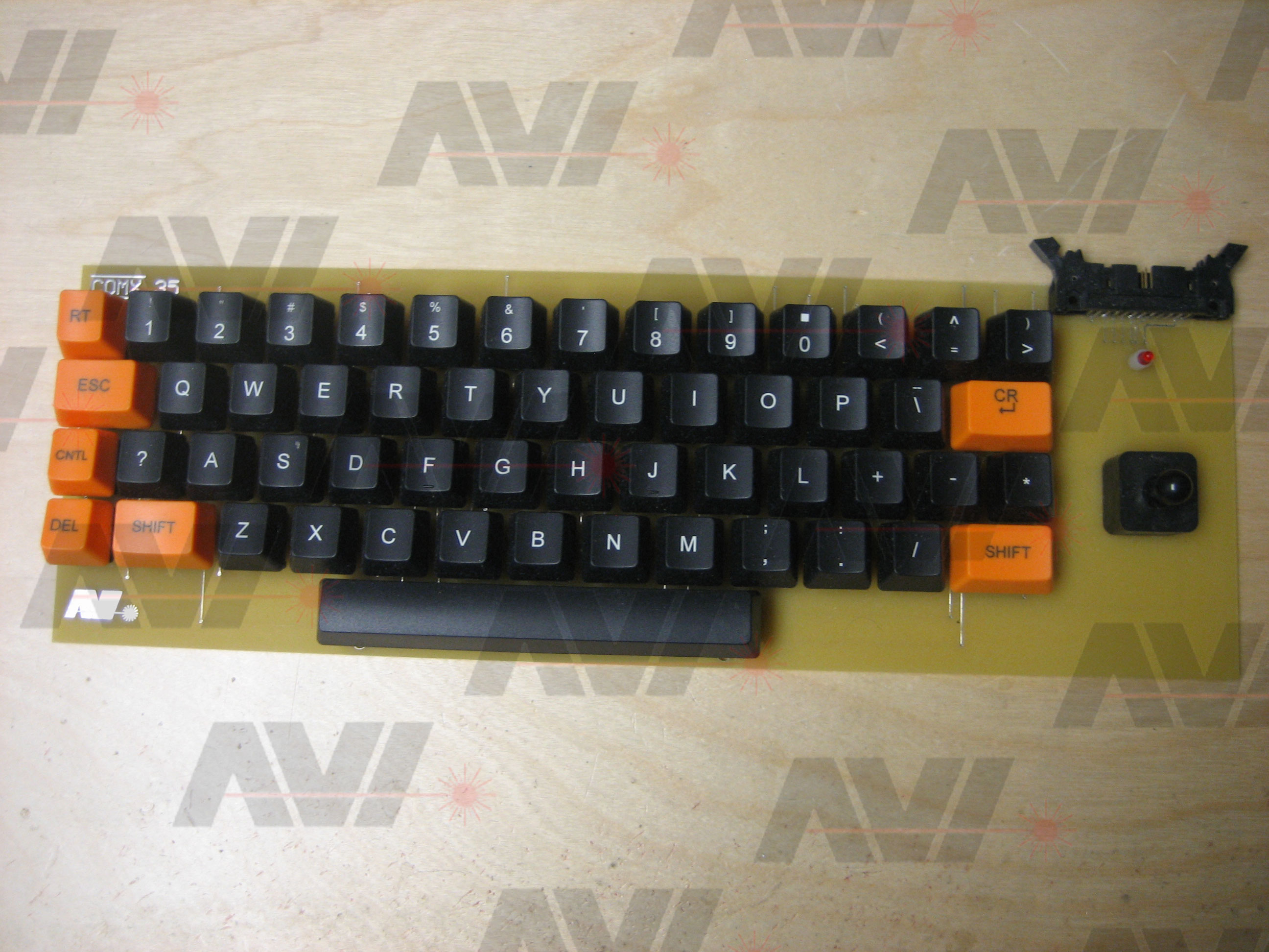
I used some of the extra keycaps I had made for the VIP II keyboard. I made stickers for some of them so they would indicate the correct COMX functions. Some of the shifted keys are still incorrectly labeled, but this is so much better.
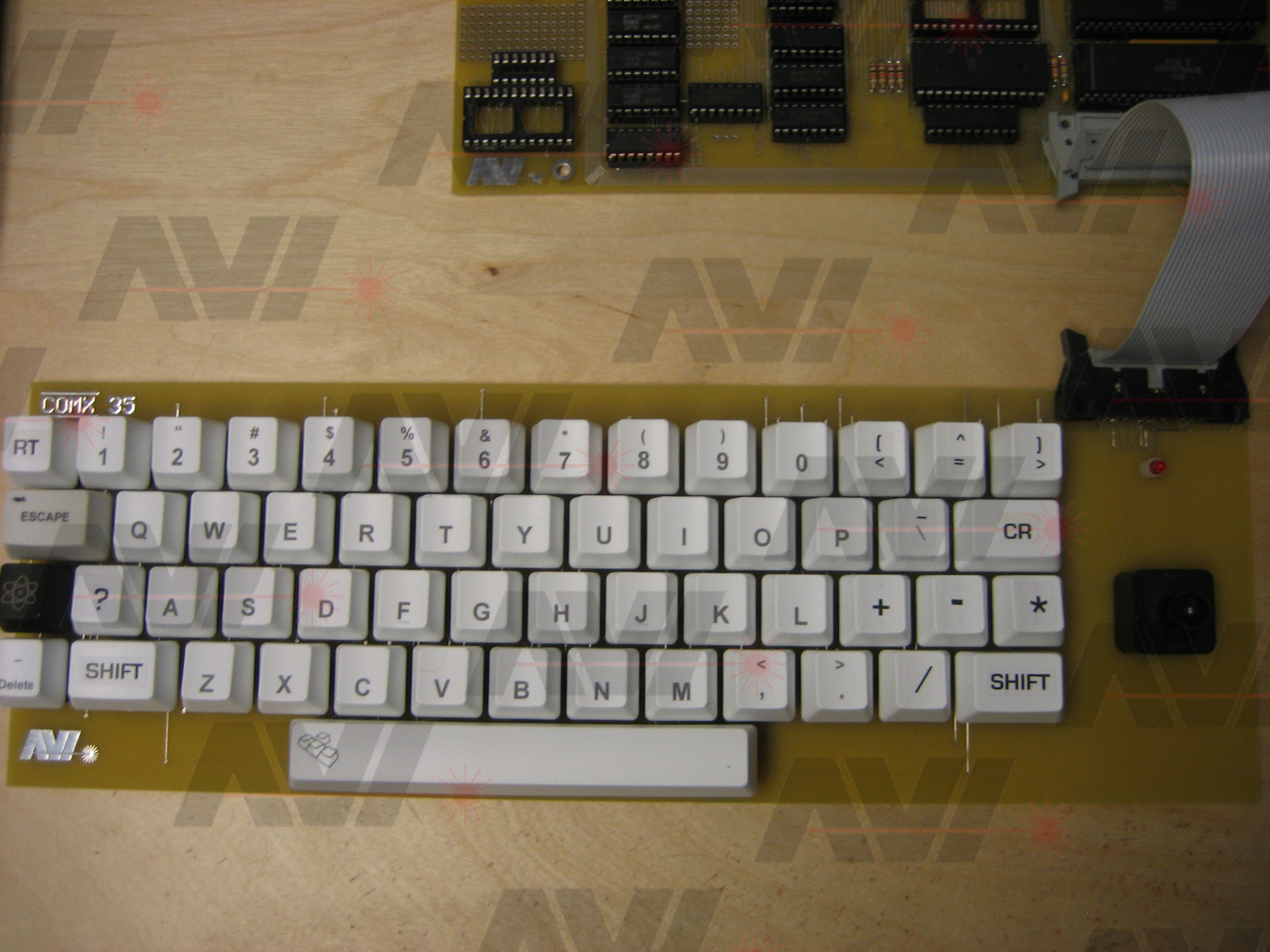
Here are pictures of the system:
Here is a better picture of the joystick on the keyboard PCB:
All the keys functioned as they should, even though some had incorrect markings. The joystick also worked as it should.
KEYCAPS
I needed a set of correctly labeled keycaps that matched the colors of the original COMX keyboard, so I had some custom keycaps made. I used the keycap designer at WASD Keyboards (http://www.wasdkeyboards.com/index.php/wasd-v1-custom-keyboard.html). Since some of the keys on the COMX don't match the available sizes for a standard PC keyboard, I made some substitutions and ordered a couple standalone keycaps.
Here is how the keyboard came out:
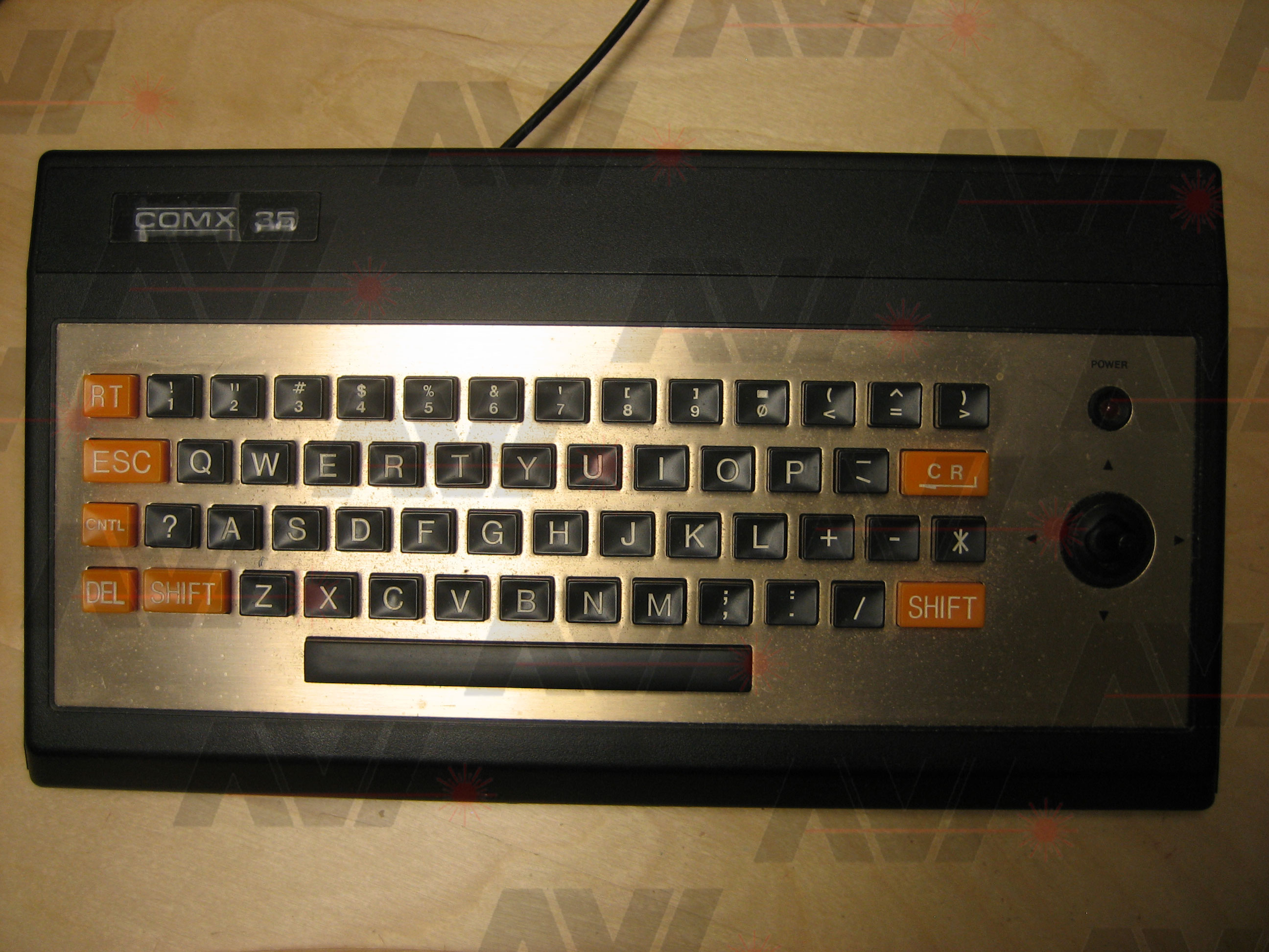
Here is what the original COMX-35 keyboard looks like:
NTSC / PAL SELECTOR
To complete the project with all the additions I wanted, all that was needed was a way to select between the PAL and NTSC video standards.
As I said before, my version of the COMX-35 was designed to be PAL. I did this for two reasons. First, it would be easier for me to trace out problems with the schematic of the original COMX-35 I drew. Second, custom crystals are expensive.
When I stripped the dead COMX, I saved the two crystals and used them on the board I built.
The PAL crystal frequencies were 8.867MHz and 5.626MHz.
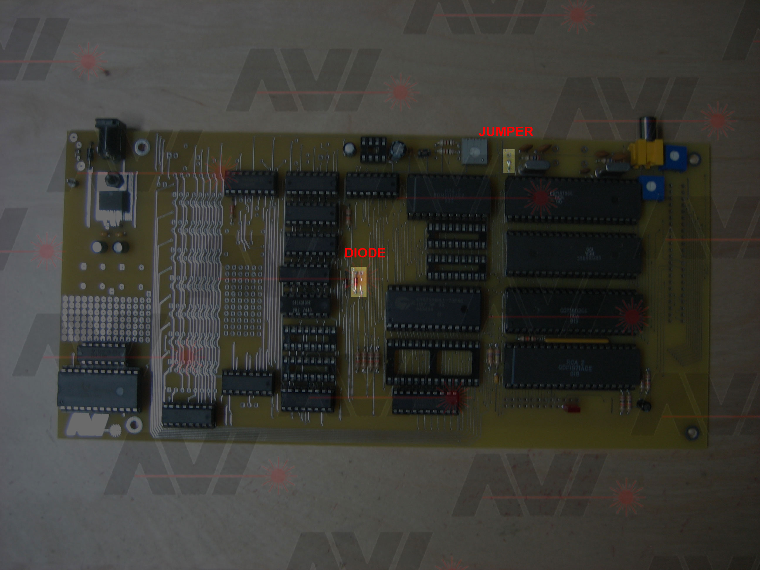
To convert a PAL COMX-35 to work with an NTSC monitor, the following must be changed:
- A diode must be removed
- Another diode installed
- A pin on the CDP1870 chip must be moved to ground or +5 Volts.
- The PAL crystals (8.867236MHz & 5.626MHz) need to be replaced with two different frequency crystals (7.15909MHz & 5.67MHz)
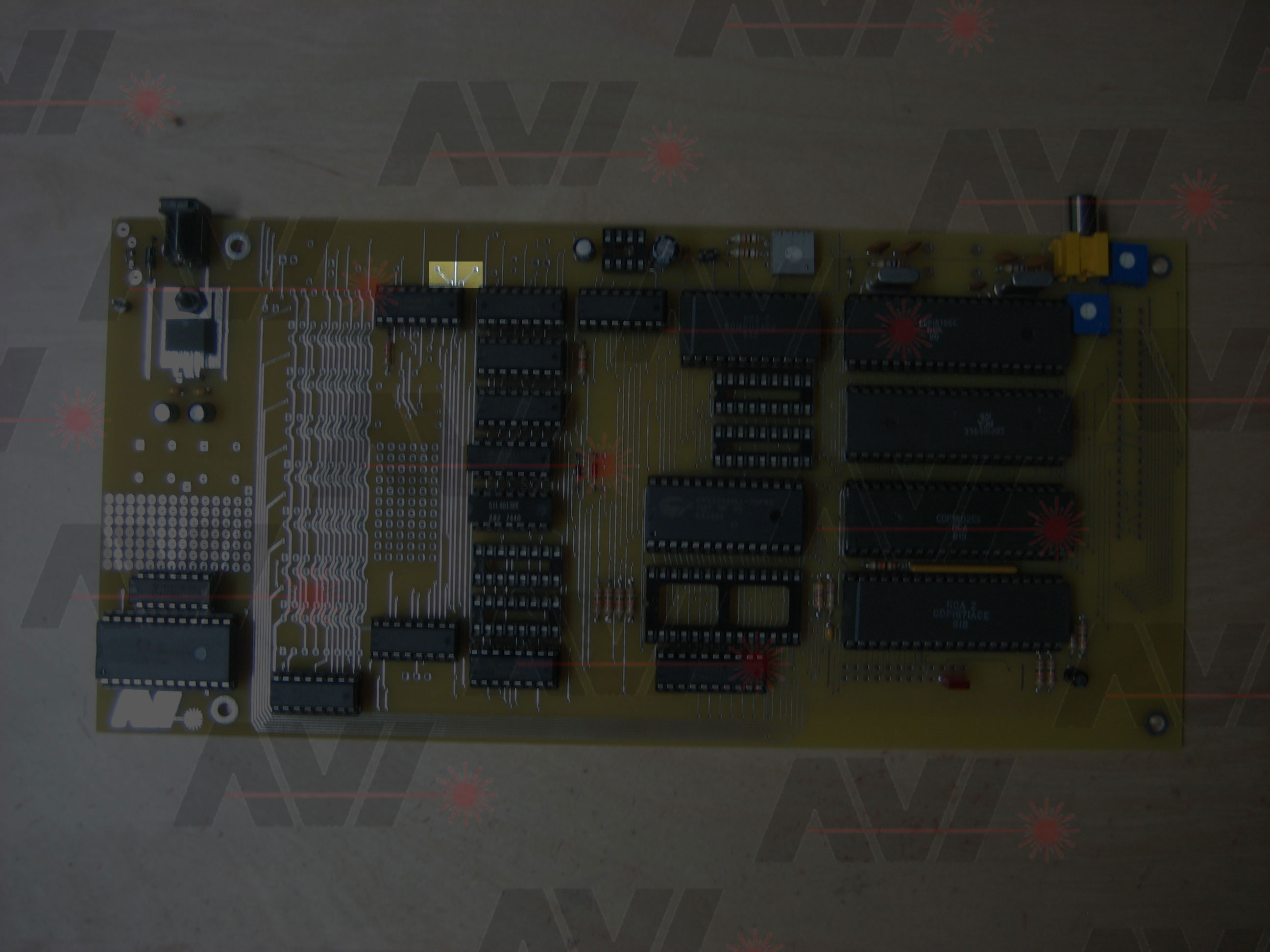
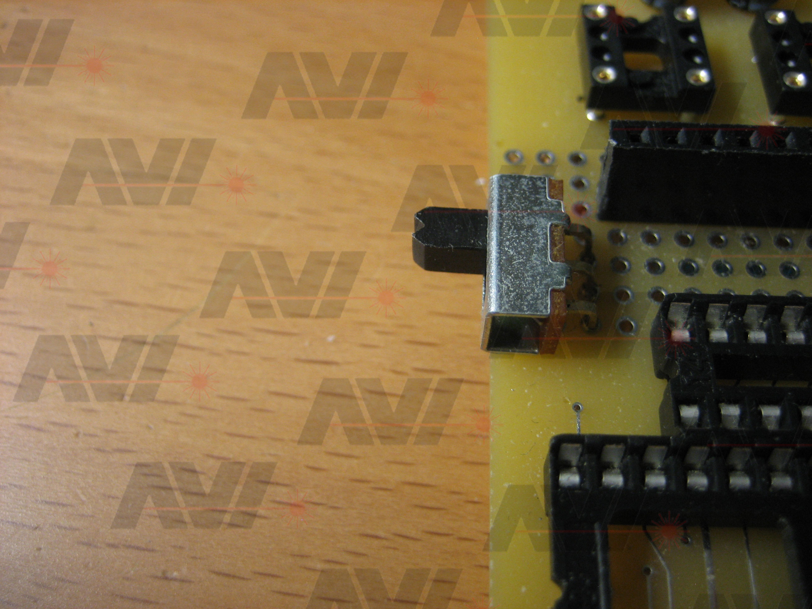
Here is a picture of the diode and jumper location:
I looked for a supplier with these frequencies in stock, but could not find one. I happen to own a Cardinal PG-3000 Field Oscillator Programmer.
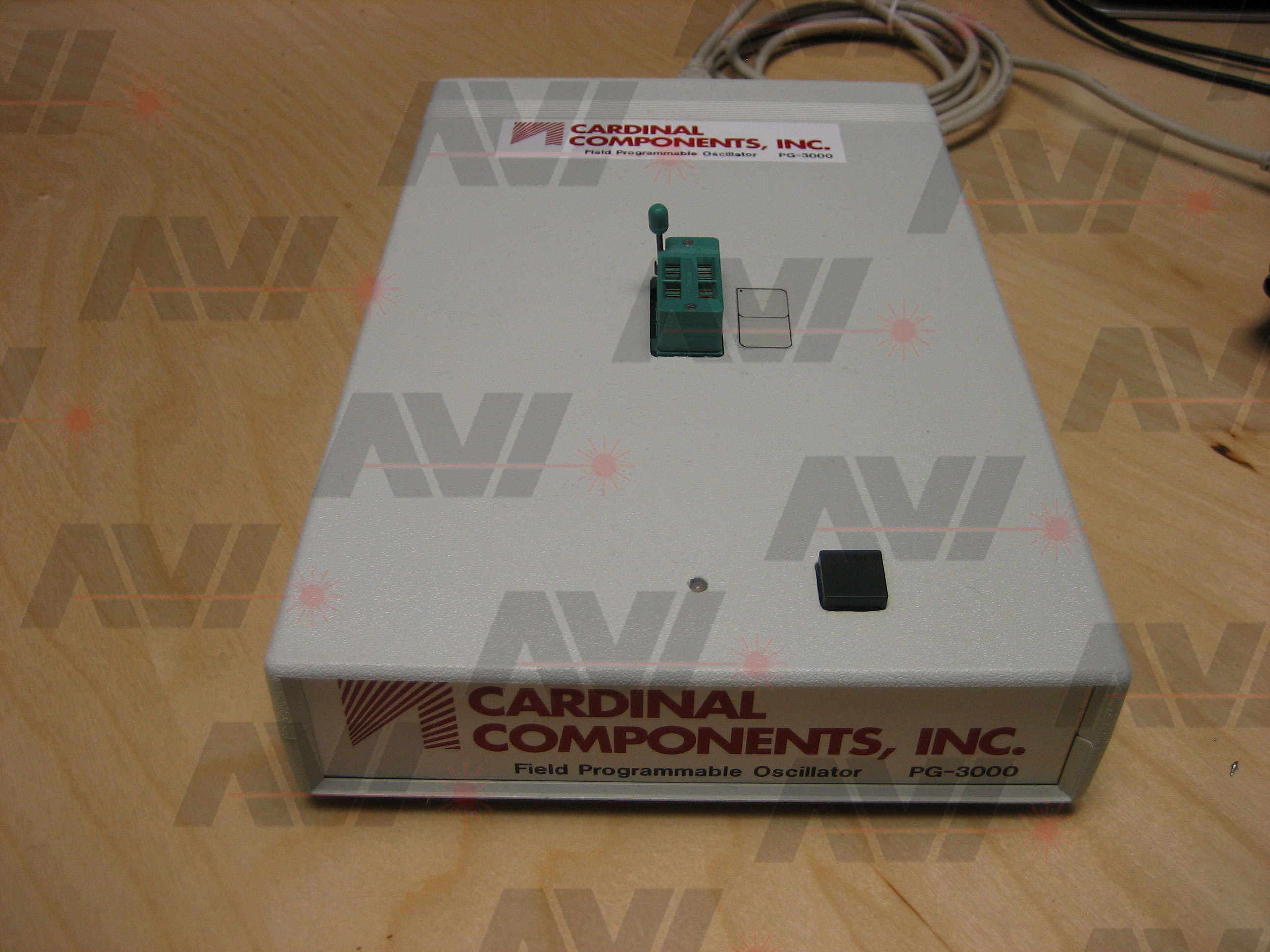
This is used to program full and half size oscillators. With this I can make an oscillator that has pretty much any frequency up to 133MHz just by programming it. The blank oscillators for this unit run around $9. Here is a link at Digikey where you can download the datasheet if you are interested (http://www.digikey.com/product-detail/en/CPPX4-A7BR/X4HS15-ND/388135).
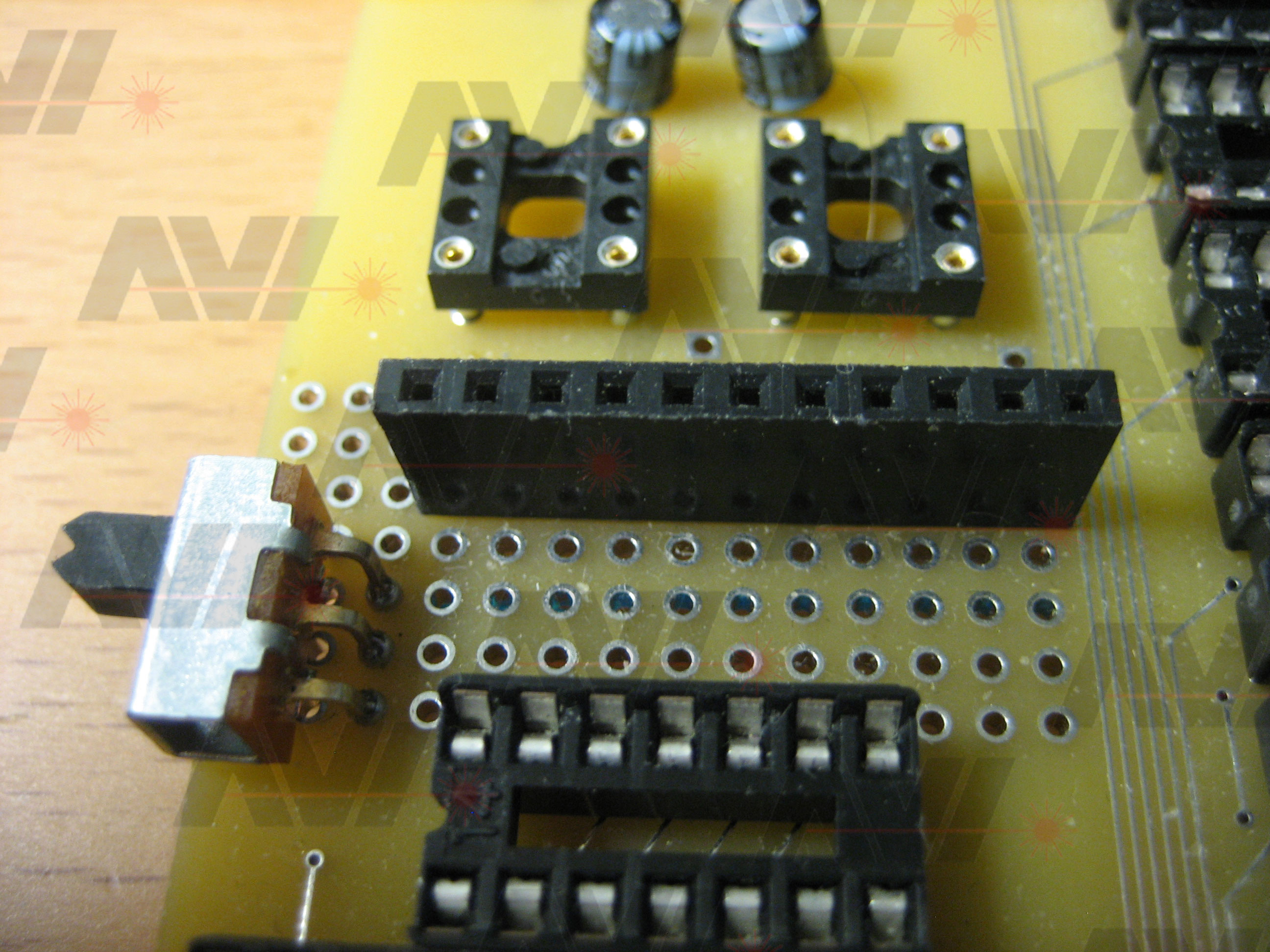
I built a little adapter board that allowed the changes outlined above to be done with a single slide switch. It isn't pretty, but it works.
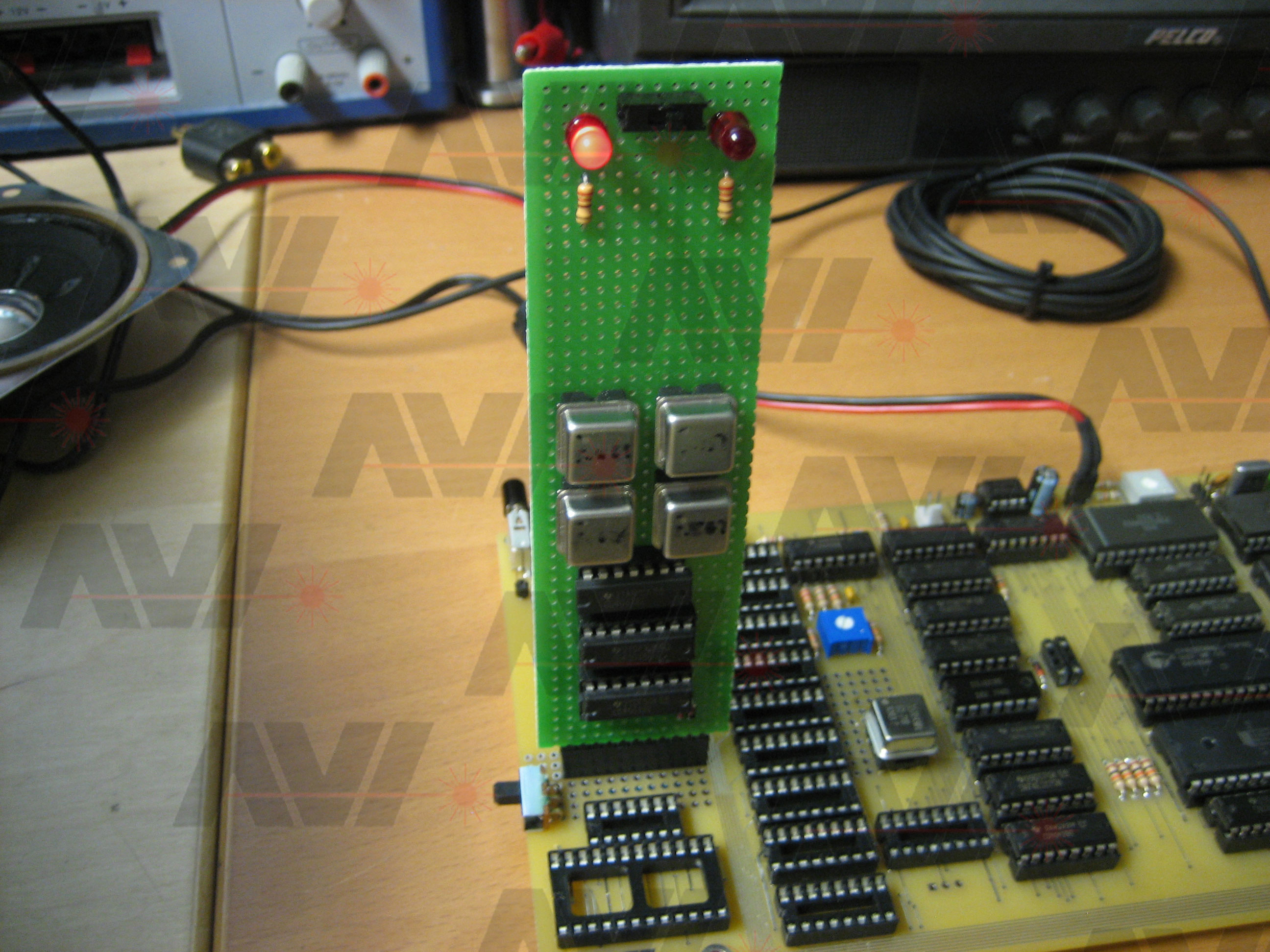
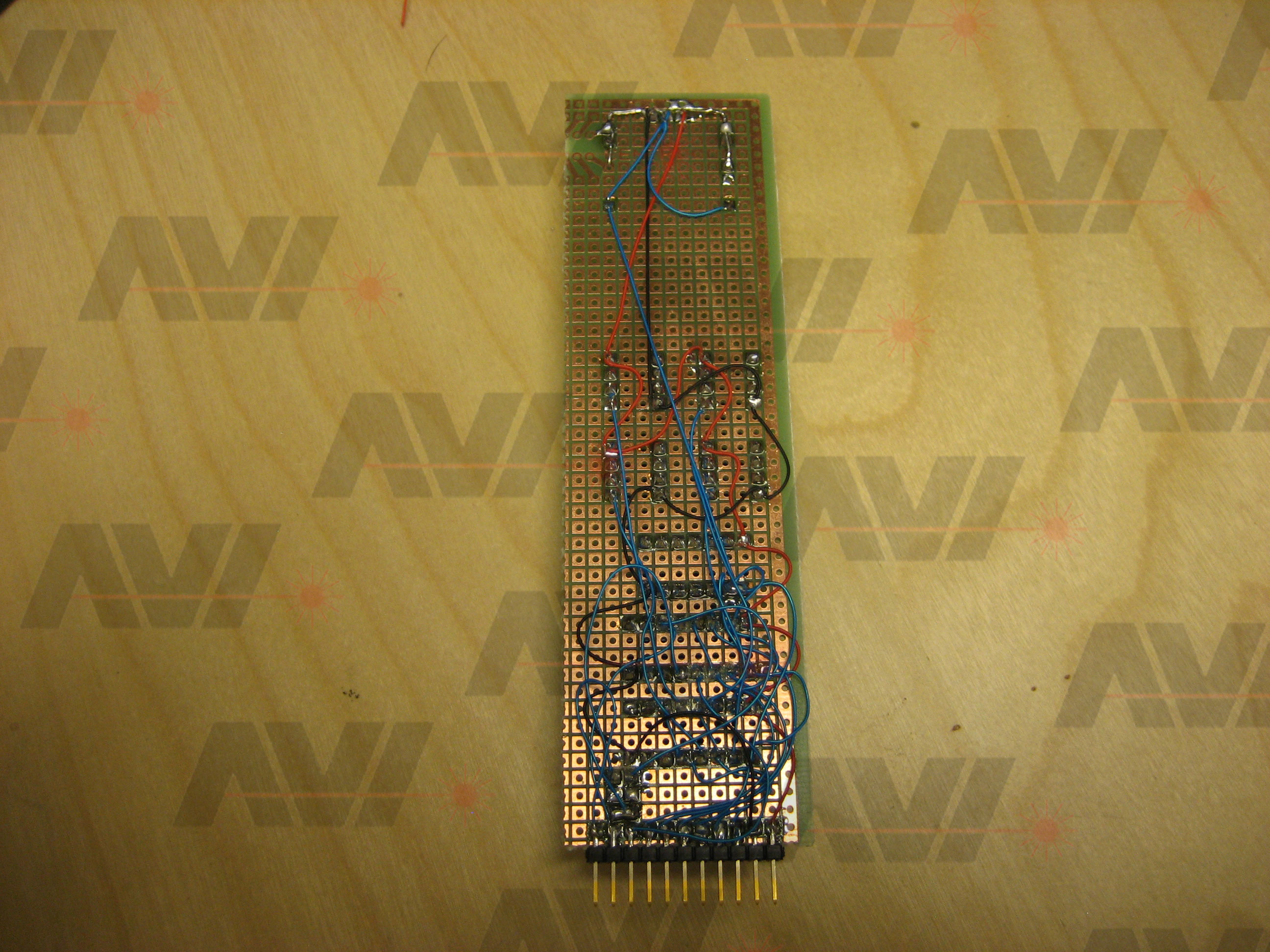
To get this to work I needed to cut the traces going to the two crystals, the diodes and the jumper. I then ran these over to a small connector I added that the selector board plugs into.
Above the connector are two oscillator sockets I had placed on the PCB for testing. My goal with them was to replace the crystals on the main board with oscillators. Here is a picture of the oscillators mounted:
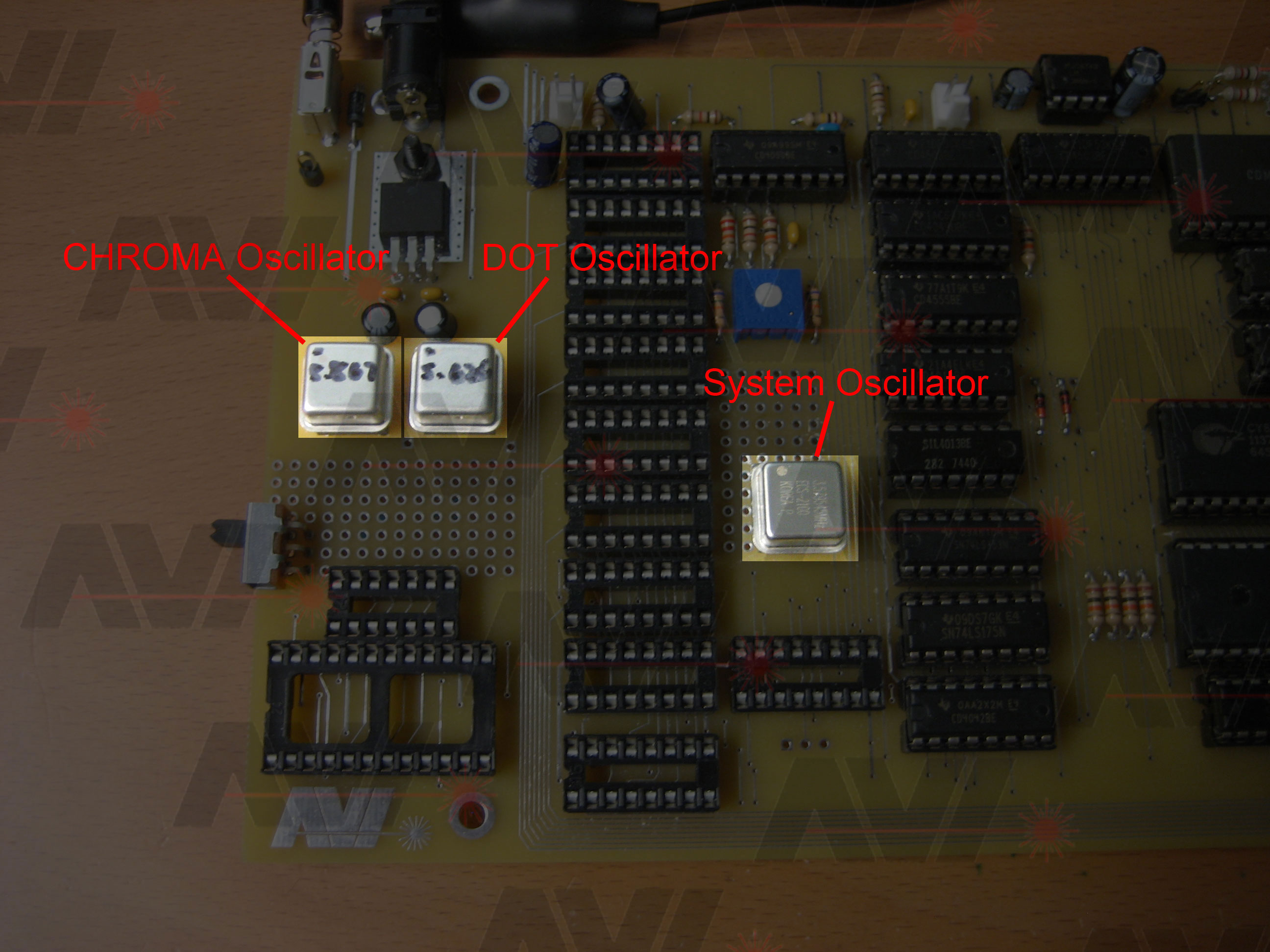
Ignore the system oscillator for now. I will cover that later.
The little green adapter board causes some jitter on the clock lines due to long, around 6 inch, wires. But since it is a proof of concept idea, I don't mind the noise on the screen. I know it will clear if I lay this section out properly.
By moving the switch at the top of the selector board, I was able to make the changes needed to swap modes. PAL or NTSC mode works fine with this modification.
I did a "PEEK(@41CA)" and was able to confirm that the board thinks it is now in NTSC mode (I got a 8 back from the peek). You can read more about the mode selection here, on page 135:
http://www.comxclub.hobby-site.com/IntroductionintoBasicProgramming.pdfHere is a picture of the system running in NTSC mode:
TURBO MODE
The 1802's clock on the COMX is driven by the CDP1870 chip. The frequency is half of the "DOT" frequency, or 2.813MHz. This is done for convenience only. The clock going to the 1802 can be higher.
As an experiment, I cut the trace going to the 1802 clock input, pin 1. I installed a color burst oscillator, 3.58MHz, on the board and wired its output to the 1802.
I plugged the Super Board (/superboard.html) into the system's expansion connector, I powered up the system and launched one of the built in games, "SPACE".
There was a noticeable increase in speed! After about two minutes the system started having issues like tearing video, sound interruptions and eventually crashing.
It took a while to figure this one out. The most notable thing was that, once again, the system worked fine when using the Fluke. I will skip the details of what I did to find the error, but I got it working.
It turns out the problem was the 1802 again. This time it was caused by me using the wrong version of the chip. I was using a CDP1802C on my board which has a maximum running frequency of 3.2MHz at 5 volts. It was trying to keep up at 3.58MHz but couldn't.
I swapped out the CDP1802C for a CDP1802ACE and the system became stable again. The chip in the 1802 POD is a CDP1802AE. That explains why it worked with the Fluke.
The CDP1802ACE has a maximum running frequency of 4 MHz at 5 volts, so it should be fine.
SQUEEZING OUT A LITTLE MORE SPEED
As another experiment to gain a faster system, I added a "Turbo Switch".
First a little background. In the COMX-35, with its Dynamic RAM, a memory refresh is required periodically to refresh the memory. This is done by a DMA OUT request that does a quick read of the location pointed to by register R0 in the 1802. After each read of the Dynamic RAM, R0 is incremented.
What the "Turbo Switch" does is break the DMA OUT line going to the 1802 causing the refresh to not happen. With Static RAM this is not a problem and is not required, until I tried to play one of the games built into the Super Board. It turns out the COMX expects the R0 counter to always increment and roll over. The COMX uses R0 as a simple random number generator.
So with planned use, I can get a little more speed out of the system by removing the memory read/R0 increment.
THE "OVERCLOCKED" COMX-35
While researching the problem I had with the CDP1802C, I noticed that the CDP1806AC had a maximum frequency of 5MHz at 5 volts. Since this was only an experiment, I programmed another oscillator at the PAL "DOT" frequency of 5.626MHz (626KHz over the rated speed specification). I used this to replace the 3.58MHz oscillator I had installed.
I powered up and everything I tried worked. I never saw an issue at this speed. Surprisingly the system runs fine at this frequency when I have a CDP1802AC installed.
I put things back the way they were, satisfied I had "OVERCLOCKED" my COMX-35.
SUMMARY
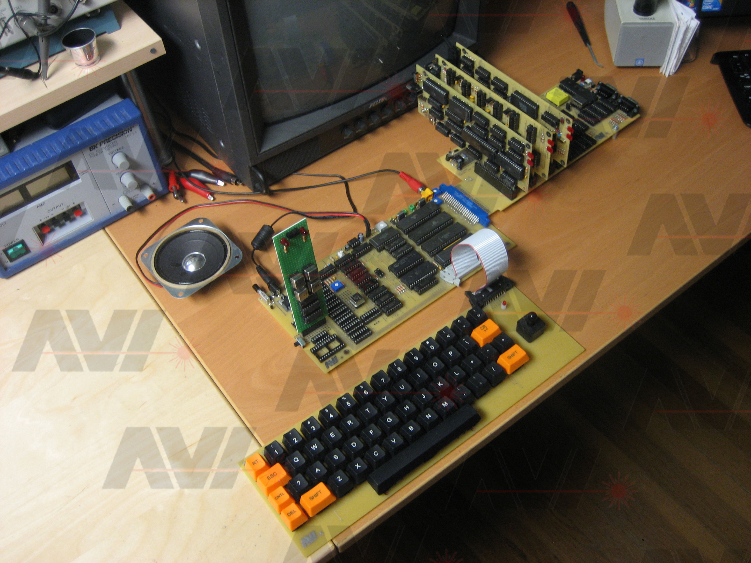
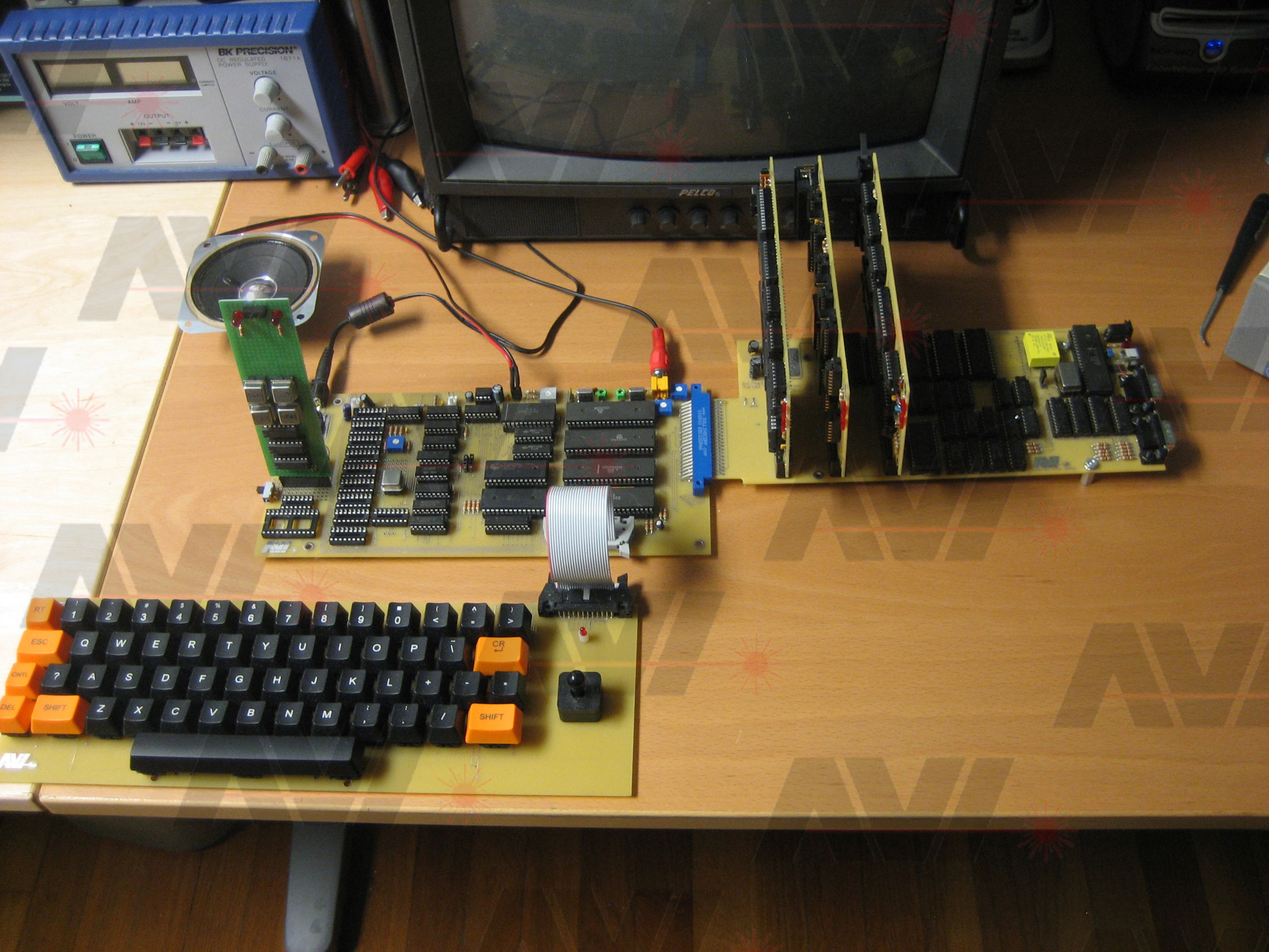
Well, that is where things stand. Here is what the final system looks like:
Here is what the final system looks like with the Super Board and three expansion cards I built installed:
I hope you found this interesting.
If you would like to discuss any of the projects on this site, or the COMX-35 itself, I have created a Yahoo Group just for that. Please feel free to visit the COMX35 Yahoo Group page located here:
http://tech.groups.yahoo.com/group/COMX35/Thank you for reading this.
ED